
The assignment for this week is to manufacture a PCB (Printed Circuit Board) using a pre-designed circuit, which is the "Hello Board" given by Daniele and the material used is FR2 (Flame Resistant 2, which is a composite made of paper and resin). We learned how to use the Eagle CAD software to export an image of the circuit for milling. The image is then processed on the Fab Modules Website to produce Gcode instructions for the specific milling machine. Afterwards, we learned how to solder components to the PCB, check the connectivity and program the on-board ATTiny45 chip using the Arduino Uno and the Arduino IDE.
We first have to pull the Fundamental2017CourseMaterial Repository to get the EAGLE board (.BRD) and EAGLE schematic (.SCH) files for the pre-designed circuit. Next, we open the board file in Eagle and click on the Layer button on top of the left hand side Toolbar:
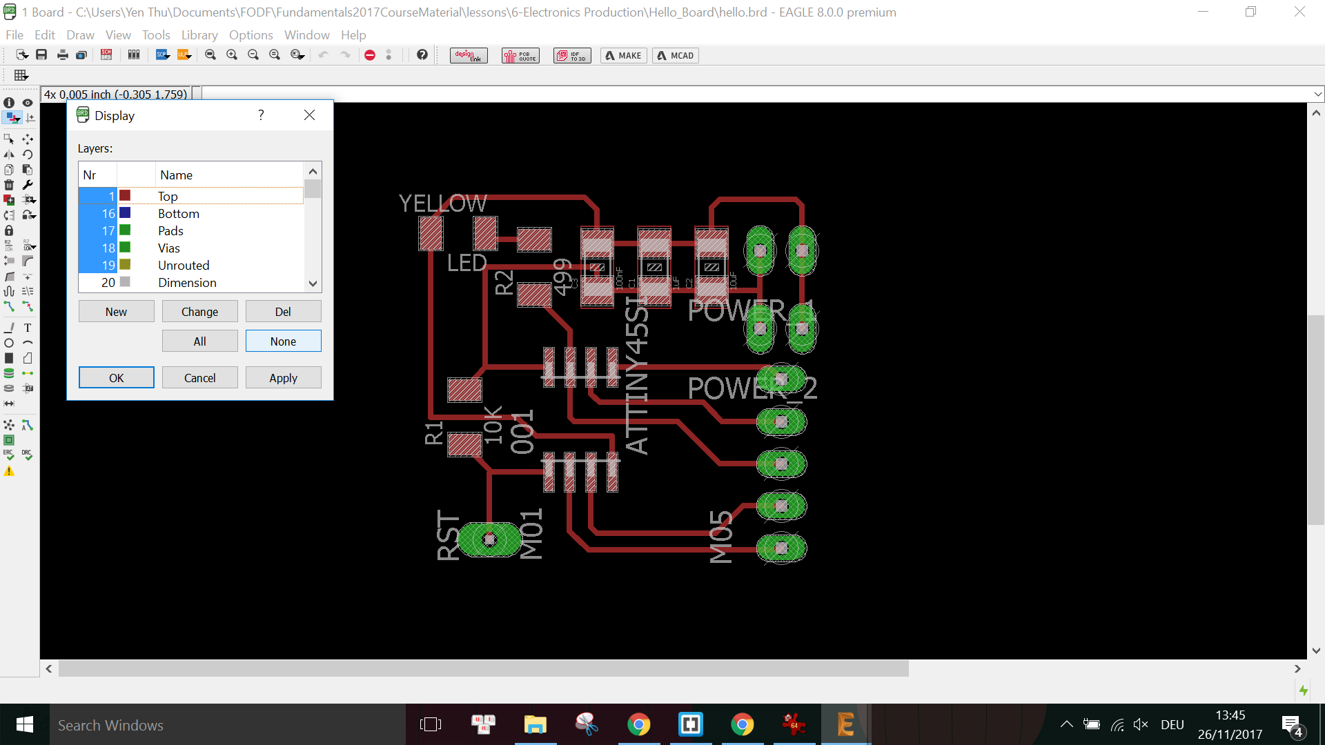
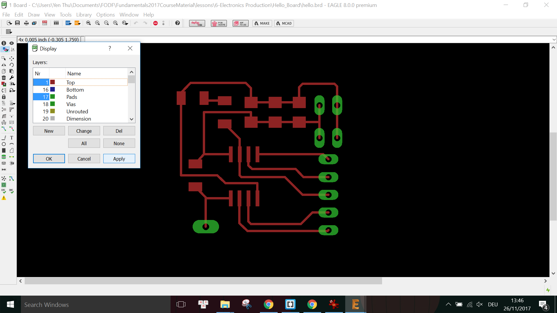
Next we click on None to deselect all layers, then click on only Top and Pads layers and finally press Apply in order to highlight only these 2 layers:
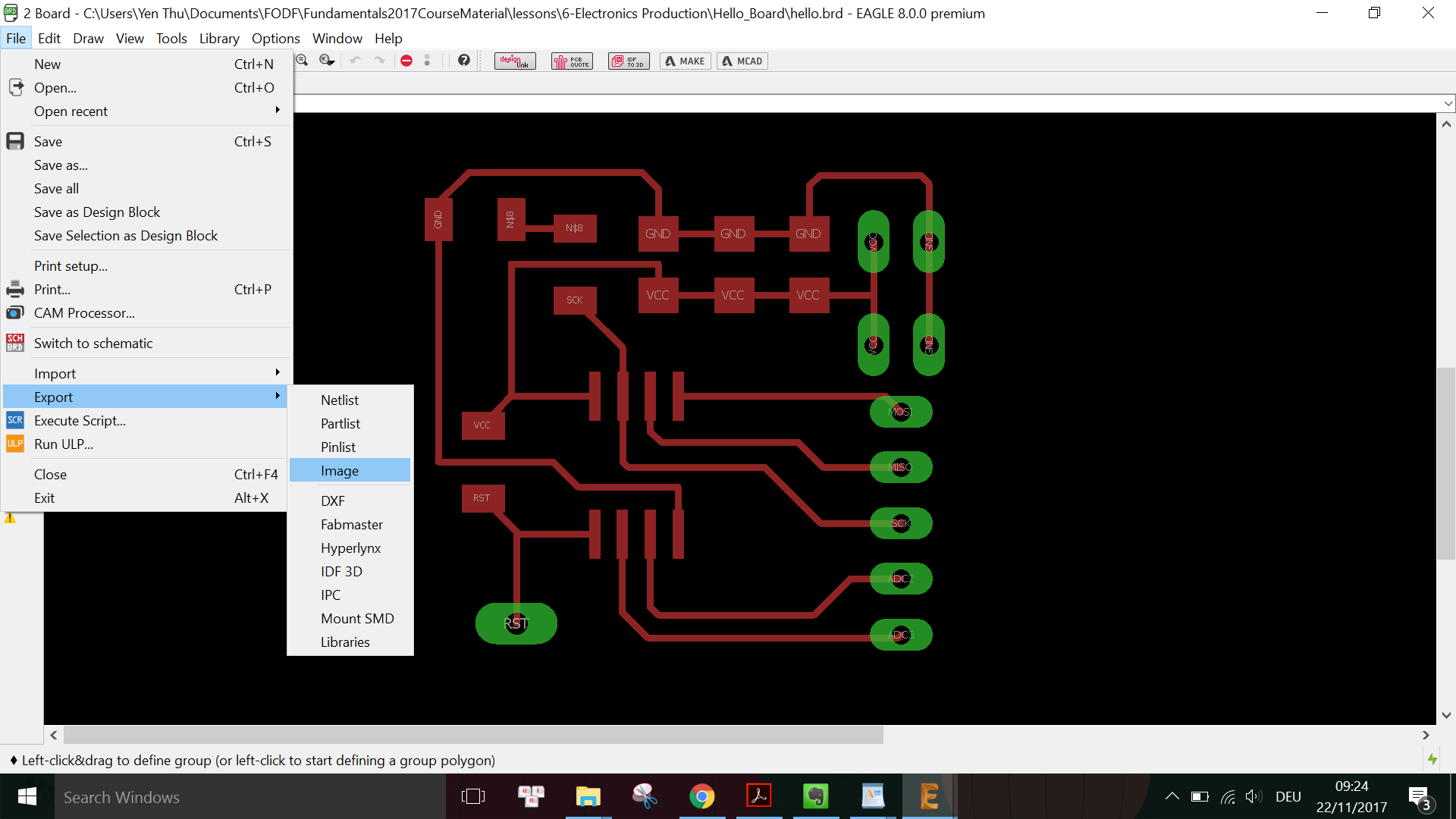
Now that we have the 2 layers needed for the milling job, we go to File -> Export -> Image in order to save an image of the circuit:
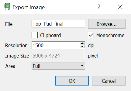
We need to specify the Resolution to be 1500 dpi, the Area to be Full and check on the Monochrome box before exporting.
And this is how my exported image looks like:
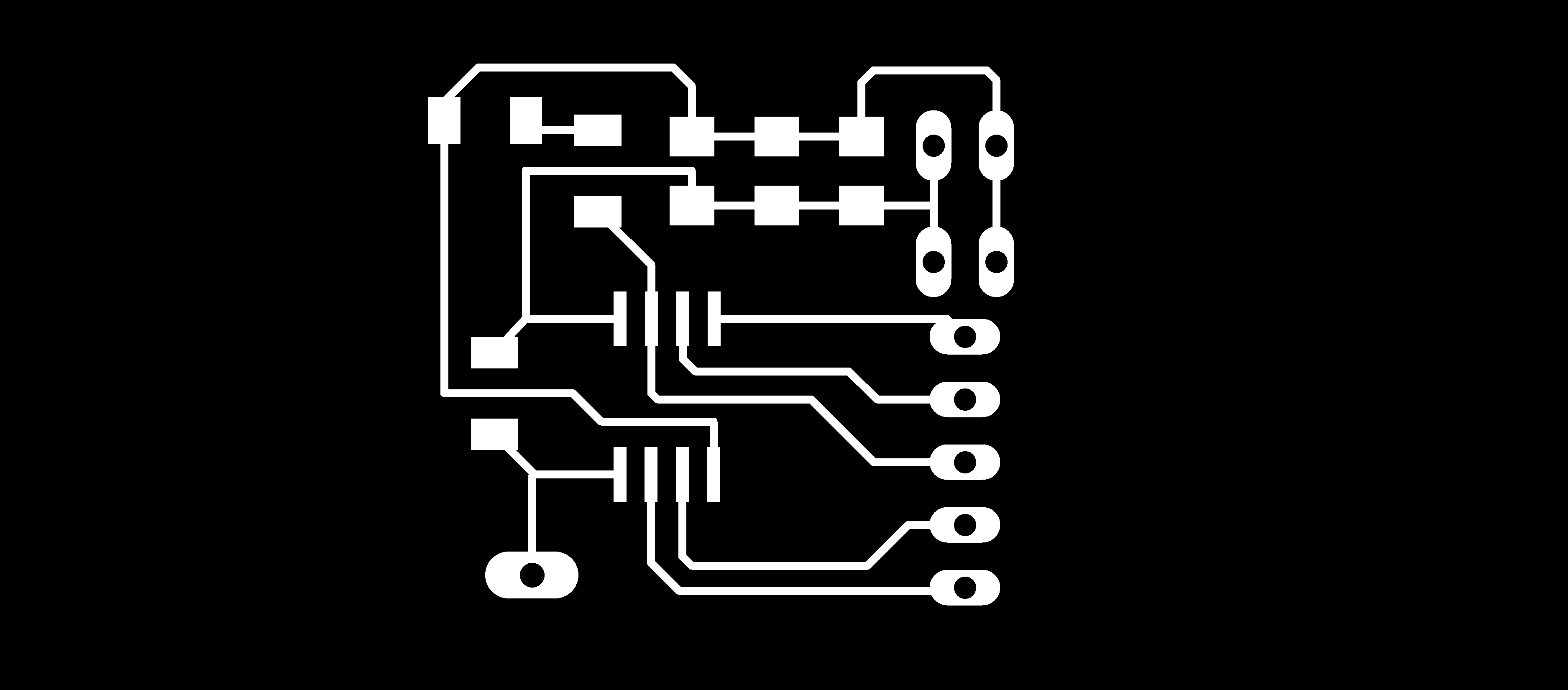
Next, we use a Photo Editing Software like GIMP to crop the image to a desired size:

After saving this new image, we have to draw the border for the circuit using a rectangular area filled with white (if the background of the image was black, and vice versa) and also save this new image to a new file:

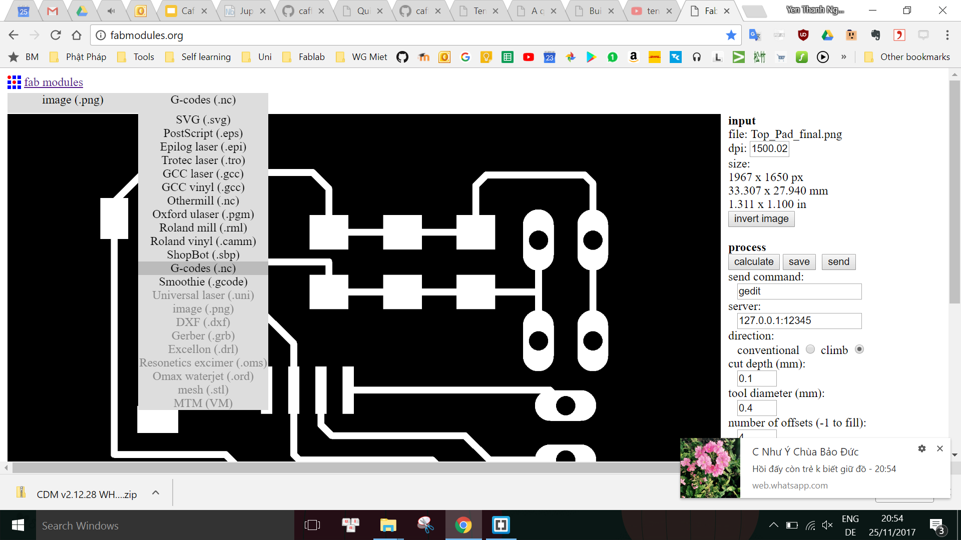
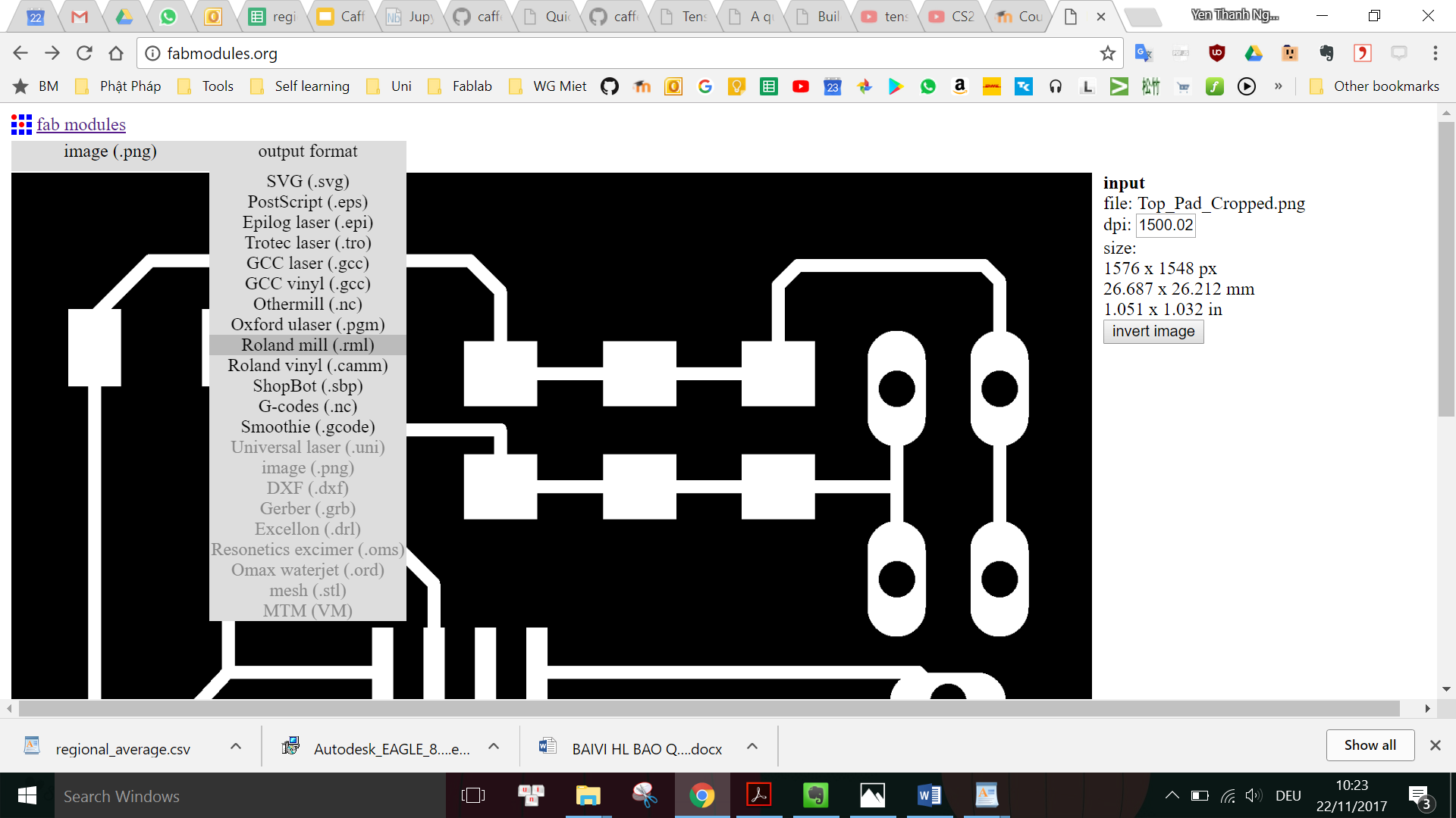
After having the 2 images for the circuit and the circuit's outine, we go to the Fab Modules Website to load the image:
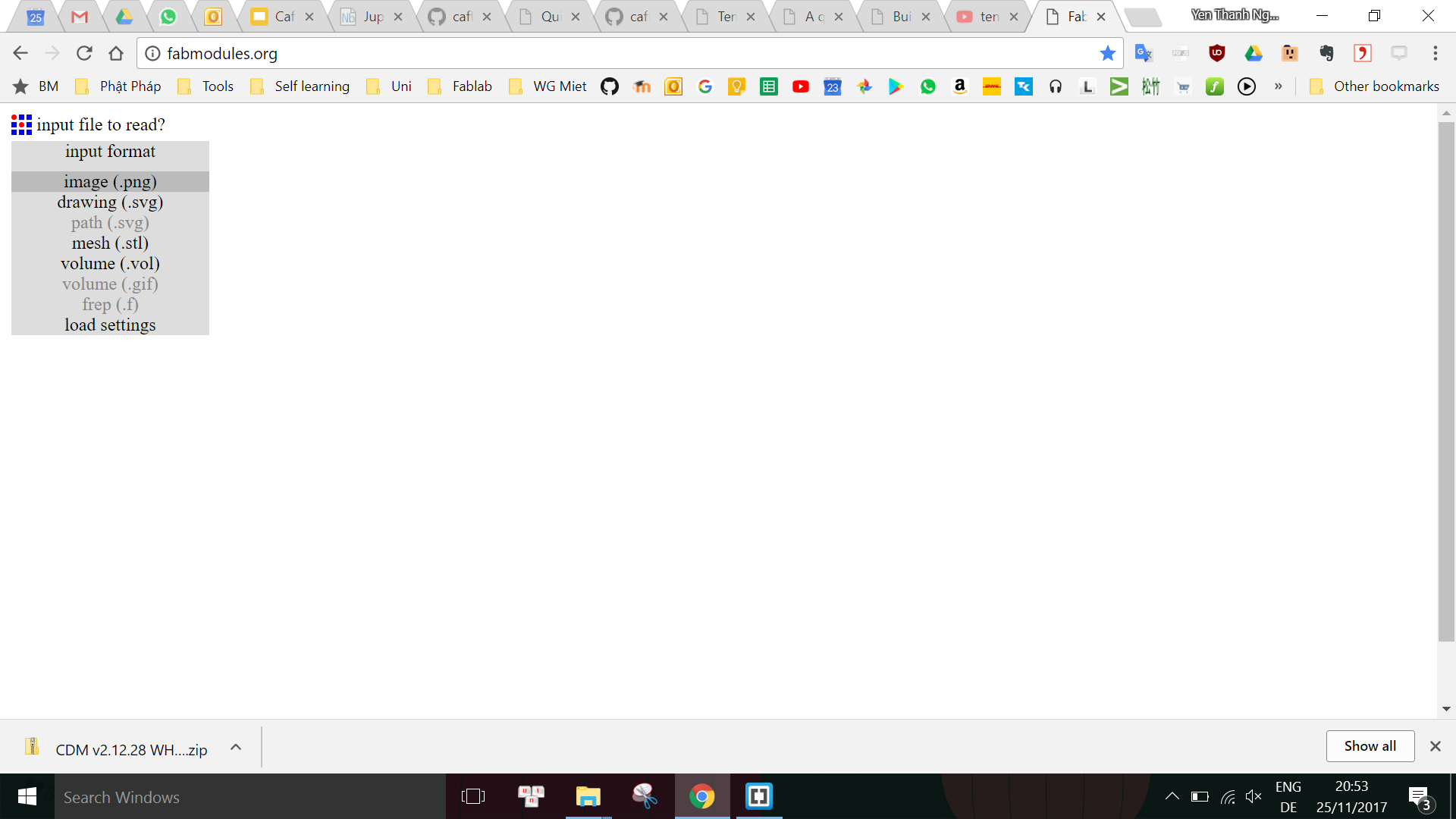
After selecting input format -> image(.png) and load the first image with the circuit traces, we need to choose the correct output format for the milling machine we are going to use. In the FabLab currently there are 2 PCB milling machines: Roland MDX-40 which is the same one that we used in last week - CNC Machining, and the Cirqoid. Thus, we have to select output format -> G-codes (.nc) if using the Cirqoid, or output format -> Roland mill (.rml) if using the Roland.
Next we have to select process -> PCB traces (1/64) in order for the program to produce toolpath for the circuit:
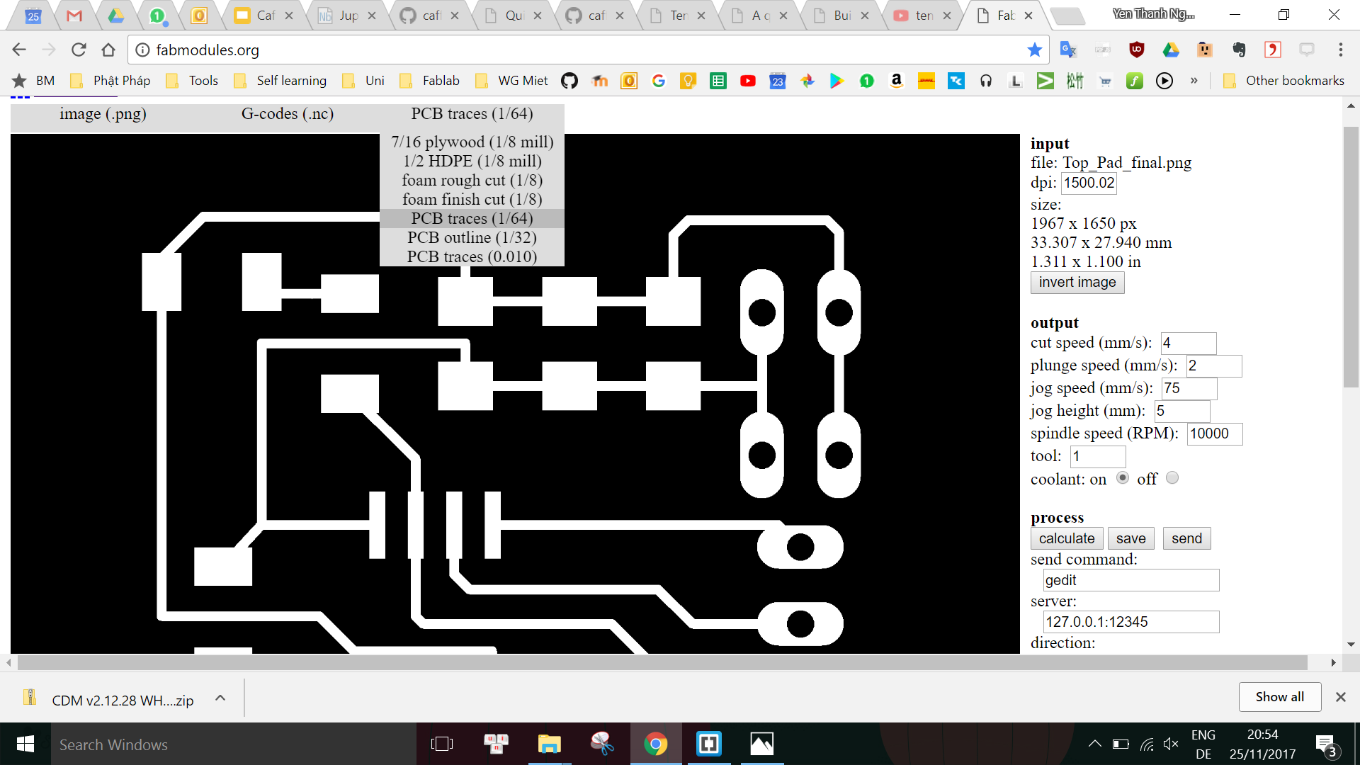
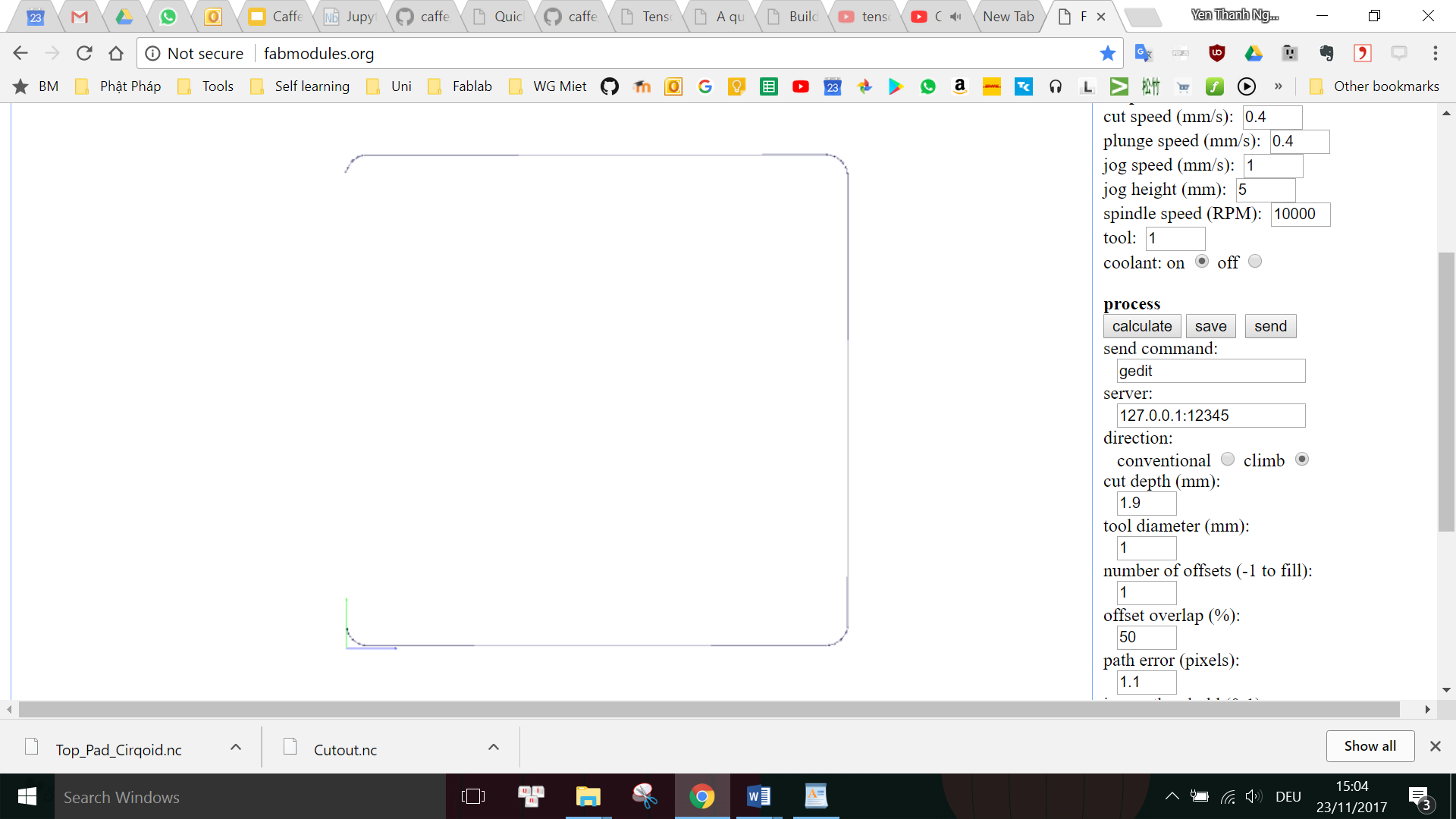
On the menu on the right hand side, we have to input the parameters for the milling job depending on the type of machine selected. Since we have already worked with the Roland last week, this week I would like to try working with a new machine so I use the settings for the Cirqoid (which are provided by Daniele) as followed:
                        - cut speed 1mm
                        - plunge speed 1mm
                        - jog speed 1mm
                        - jog height 2mm
                        - cut depth 0.0mm
                        - tool diameter 0.2mm
                        - offset overlap 55%
                        - number of offsets 4
Note that the cut depth is 0.0 because according to Ahmed, the thickness of top copper layer is only 0.0345 mm and later on we are going to set the Z-origin to be just touching the copper surface.
After filling in the correct settings, we click on Calculate so that the program can generate toolpath for the machine:
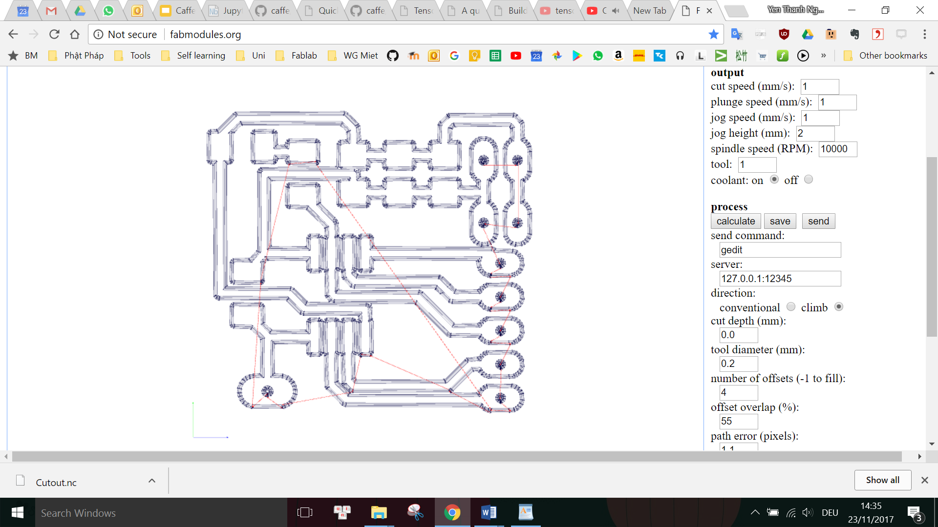
Since these are only traces of the circuit, we have to save this job and then generate a new job for cutting the board's outline using the other image and the same process:
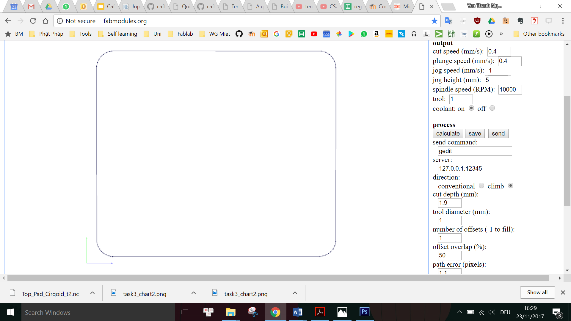
However, the settings for this job is different because this time we are not only milling out the top copper layer but we need to fully cut through the FR2 material:
                        - cut speed 0.4mm
                        - plunge speed 0.4mm
                        - jog speed 1mm
                        - jog height 5mm
                        - cut depth 1.9mm
                        - tool diameter 1mm
                        - number of offsets 1
Again, we save this job and proceed to the milling machine for manufacturing the PCB.
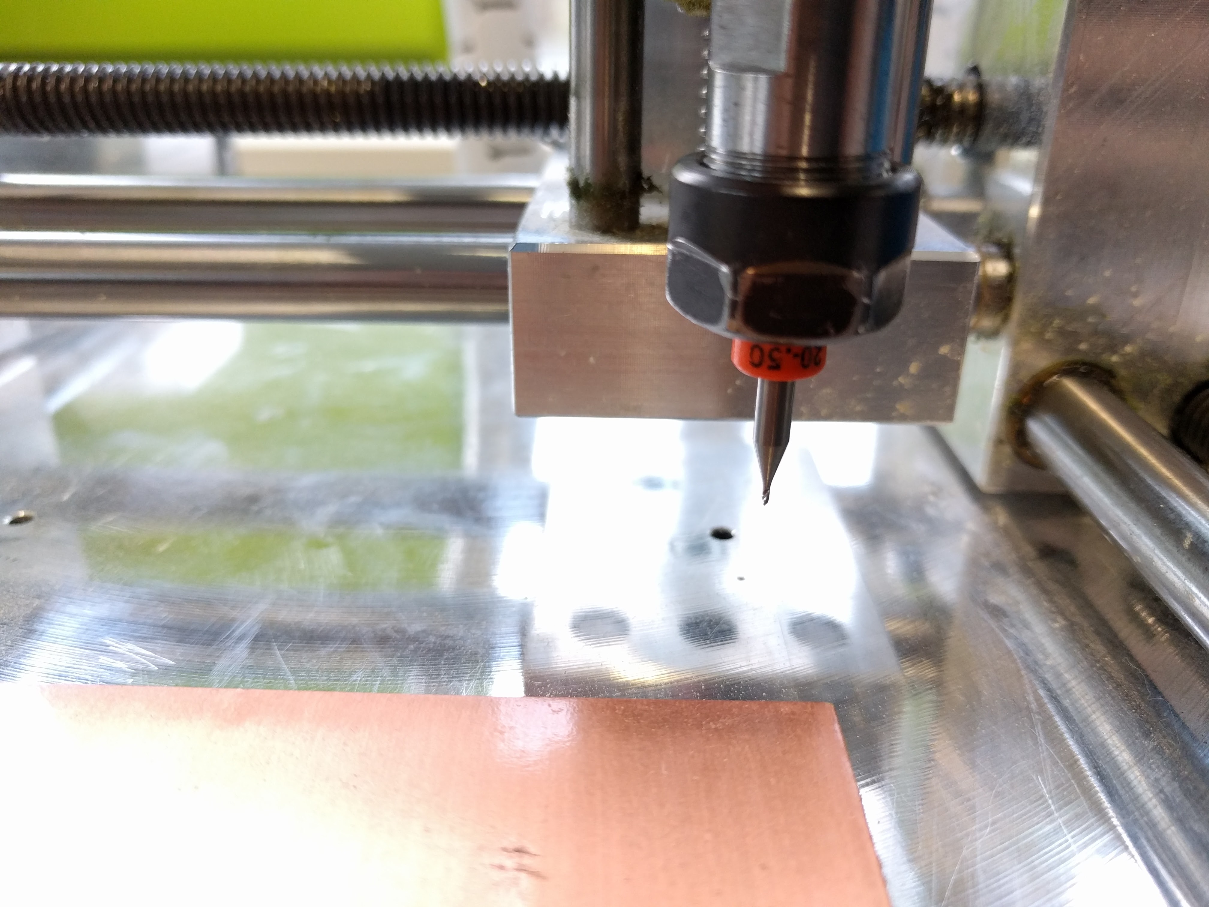
First, we have to fix the PCB on to the machine's bed (which has been prepared for us by Daniele) and then insert the correct tool. For the trace milling job, as seen in the first settings, we have to insert 0.2mm milling bit into the spindle:
Next, we have to open the dedicated software and connect the computer to the milling machine and press $H to home the machine. Now it is time set the XYZ origin point for the milling job. The origin point in the FabModules CAM processor starts from the bottom left of the circuit's image, thus, we need to set the origin point also at the bottom left of the region we want to mill.
First we raise the spindle in Z direction so that it is at a safe distance (about 5mm) above the copper surface, then we use the X-/X+ or Y-/Y+ buttons to move the spindle to desire XY-origin. The tough part is to set the Z-origin so that it is not too deep into the material or too far away from the copper surface. At the distance of 5mm above the copper surface, we enter the following command into the console to enable the spindle:
M3 S100 ##to enable the spindle
Then we have to lower the spindle very slowly in the Z direction, first with steps of 0.1mm, until when we are only around 1-2mm away from the copper surface, we change to steps of 0.05mm until the spindle just scratches the surface:
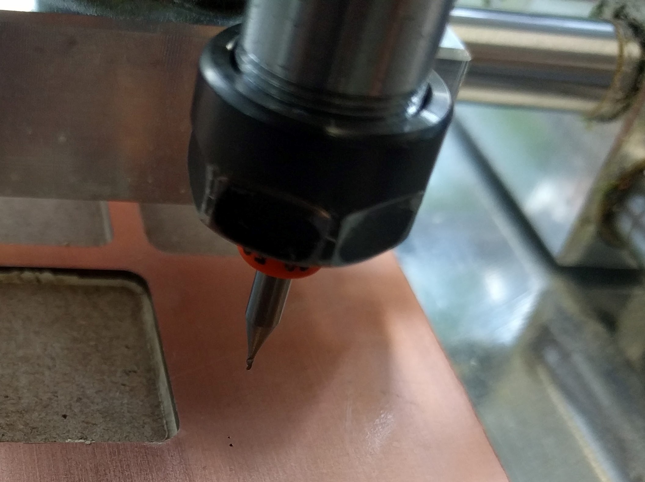
In the image above, the first time I picked the Z origin it was still too deep (the point at the bottom), thus I had to redo it and the second time (the point at the top) was better.
After having the desired origin point, we press Reset Zero to set this as origin point. Then we move the spindle up in Z direction again, and stop the spindle by entering in the console:
M5 ##to stop the spindle
Now we can load the G-code file for milling the traces into the software:
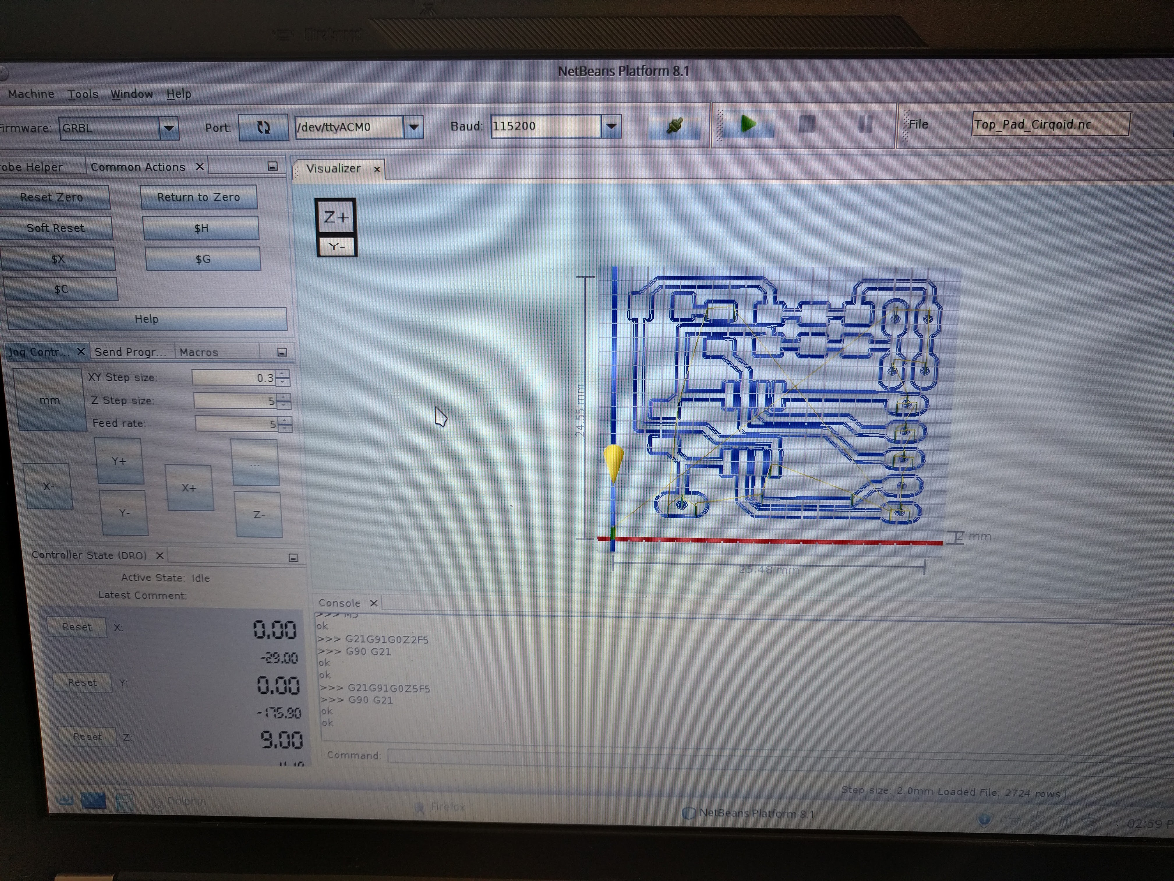
After checking that the traces look fine in the software, we can press Play to start the job, and we do not have to move the spindle to its origin position before starting.
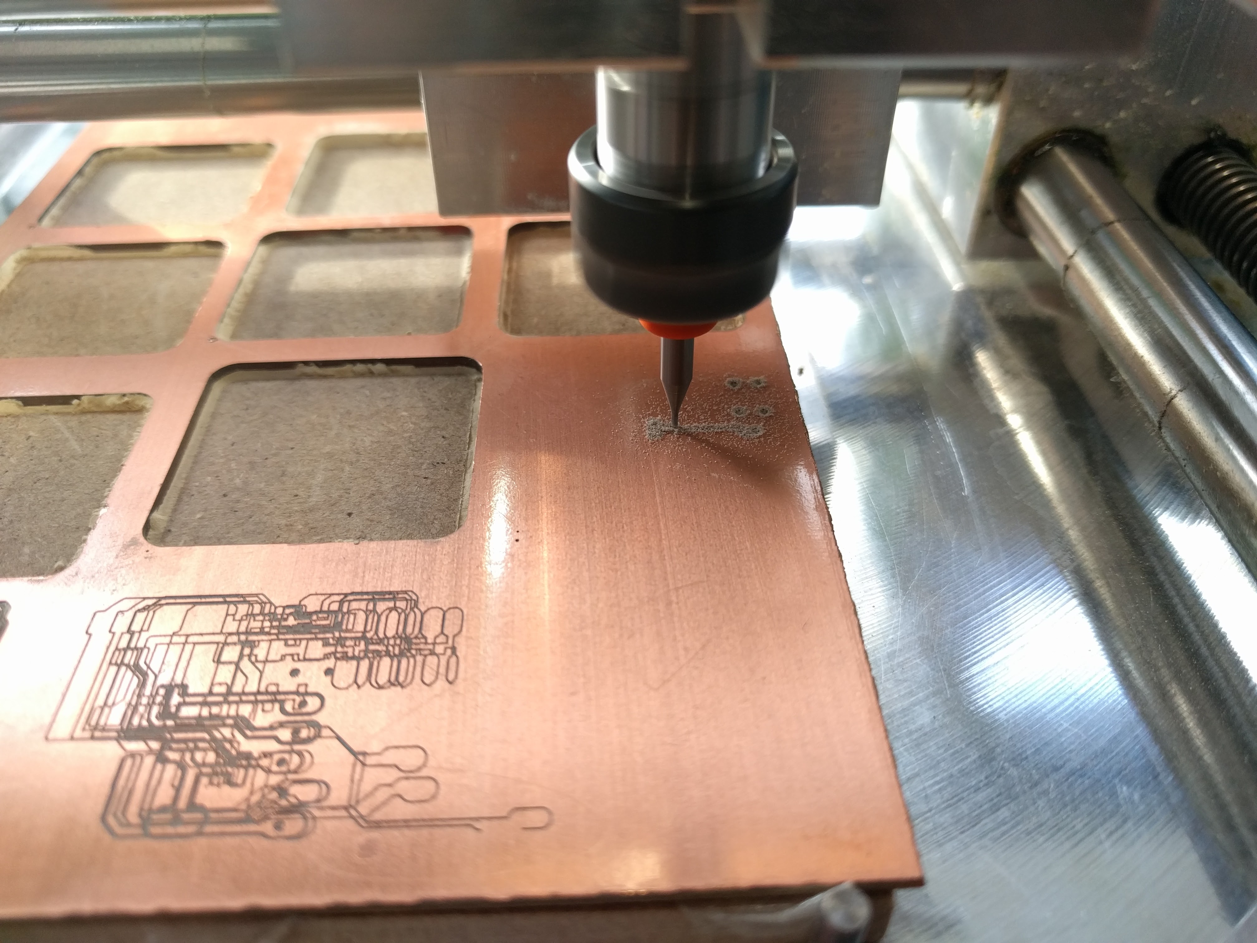
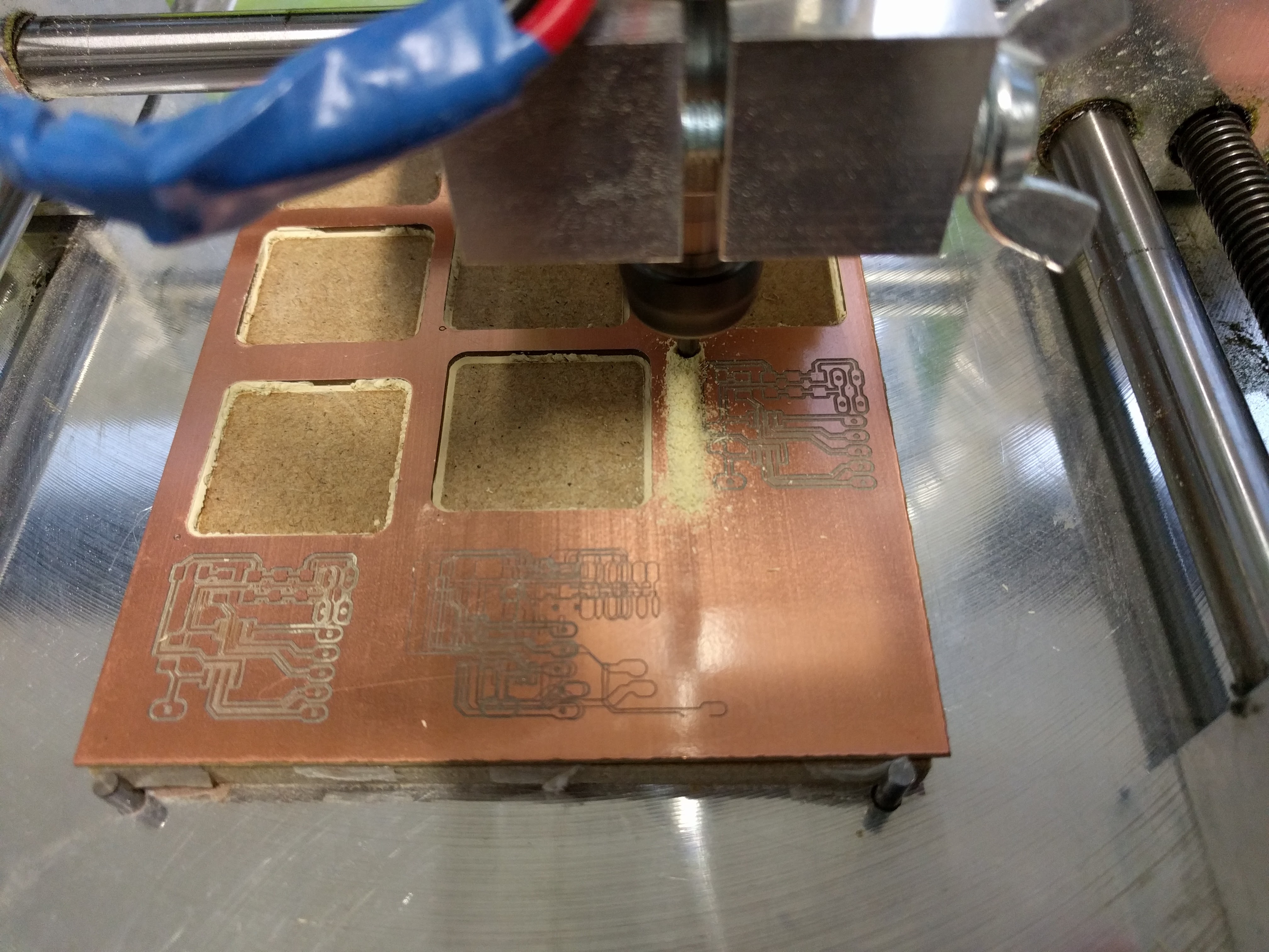
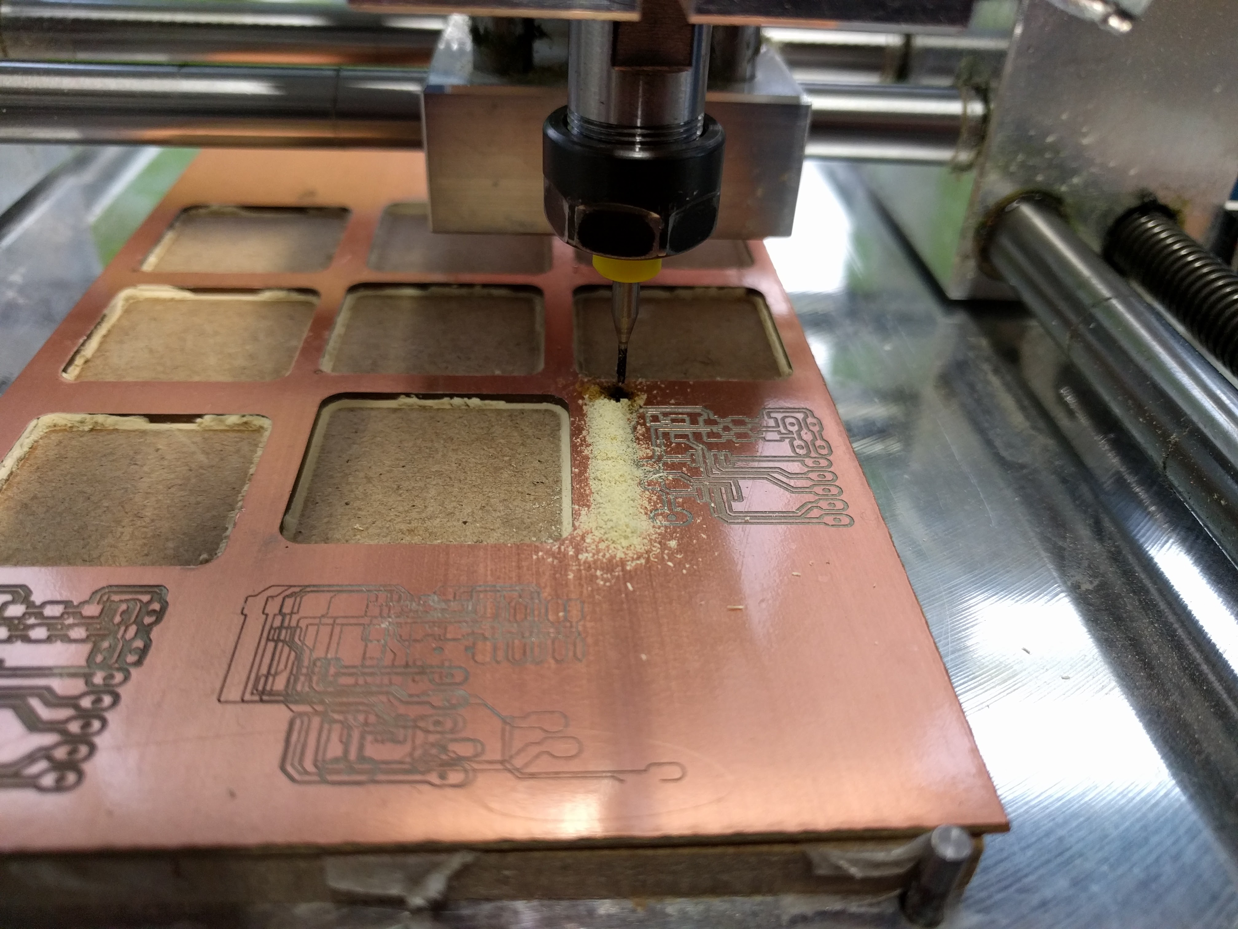
One thing to note is that we should always connect the computer to AC while the machine is milling, otherwise the computer could go to sleep after some time and the job stops in the middle of the way and we lose all information about the origin point. Here is an image of the machine while milling the traces:
When the first milling job is finished, we can use the X-/X+ or Y-/Y+ buttons to move the spindle away for viewing and for changing the tool. Note that we SHOULD NOT PRESS HOME BUTTON because this will cause us to lose the origin point of the first job.

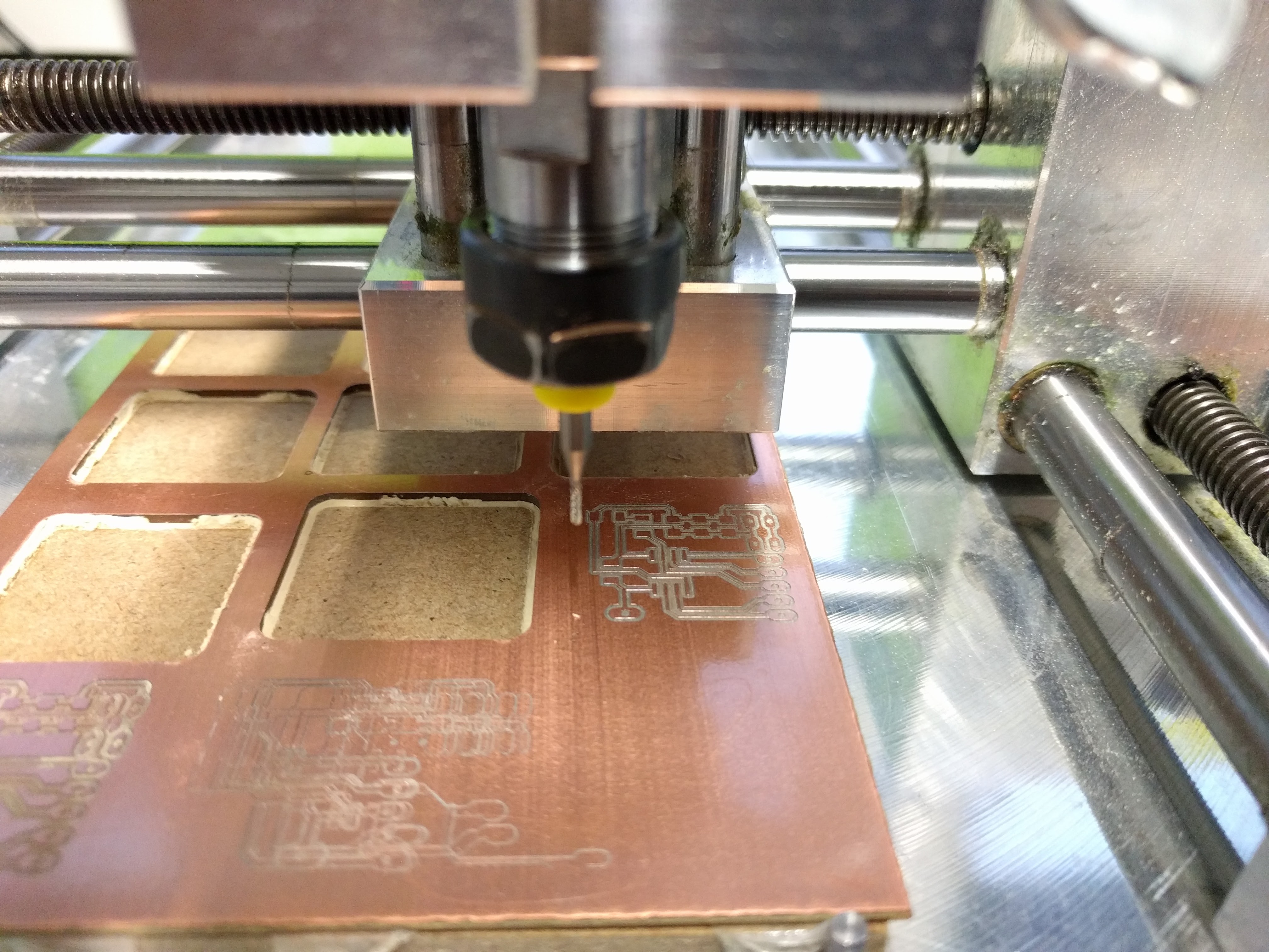
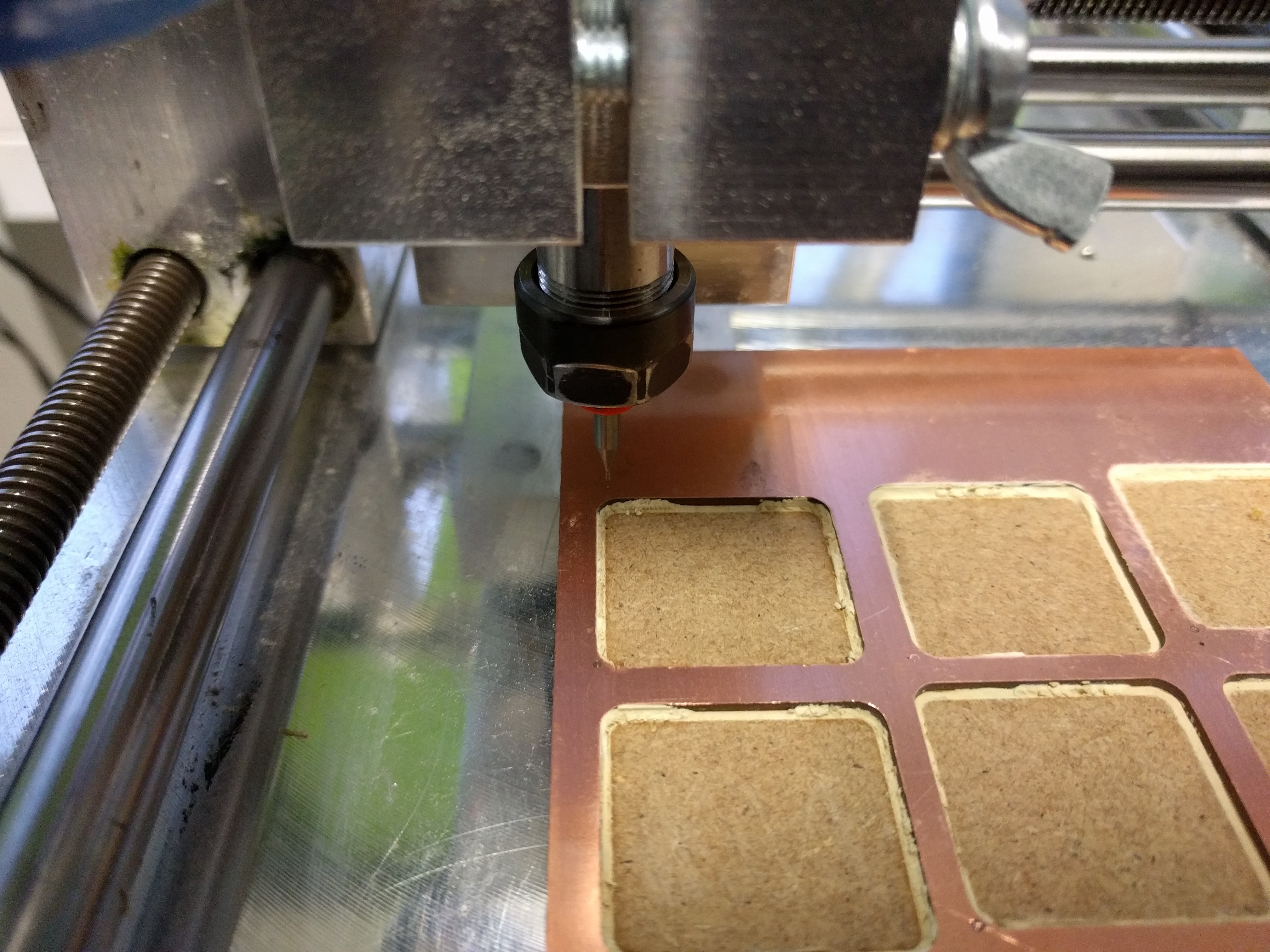
It can be seen that the traces were milling quite well. Now that I have changed to the new tool with 0.3mm diameter, I can set the new Z-origin for the second milling job without having to change the XY-origin, because only the tool length has changed. First, I have to go back to the XY-origin by entering the following commands into the console:
G0 X0    ##to move spindle to X origin
                          G0 Y0    ##to move spindle to Y origin
Now I have to set the new Z-origin using the same steps as before,
then load the G-code for cutting the outline of the board into the software and press Play again to start the job:
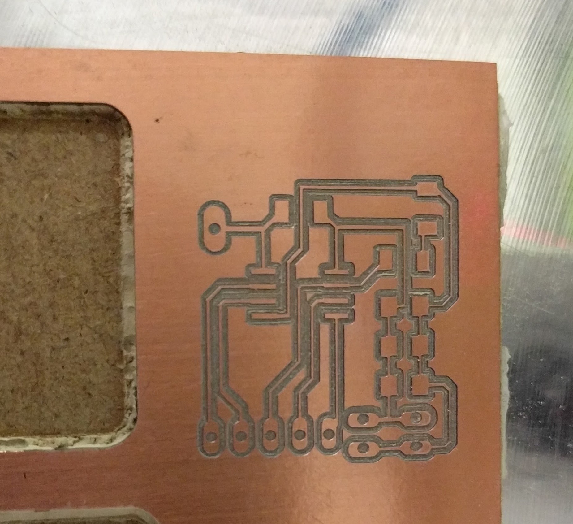
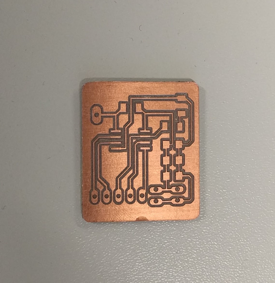
While milling my first board with the Cirqoid, I encountered a problem at this last step of cutting out the board, which will be discussed later in Section 4 - Problems and Troubleshooting. Thus, in the end my first board was missing some traces because they overlap with the outline trace:
Although these are still fixable, I still would like to make another board so that I can practice the milling procedure again. Thus, I changed the tool and started the milling job again at another origin position:
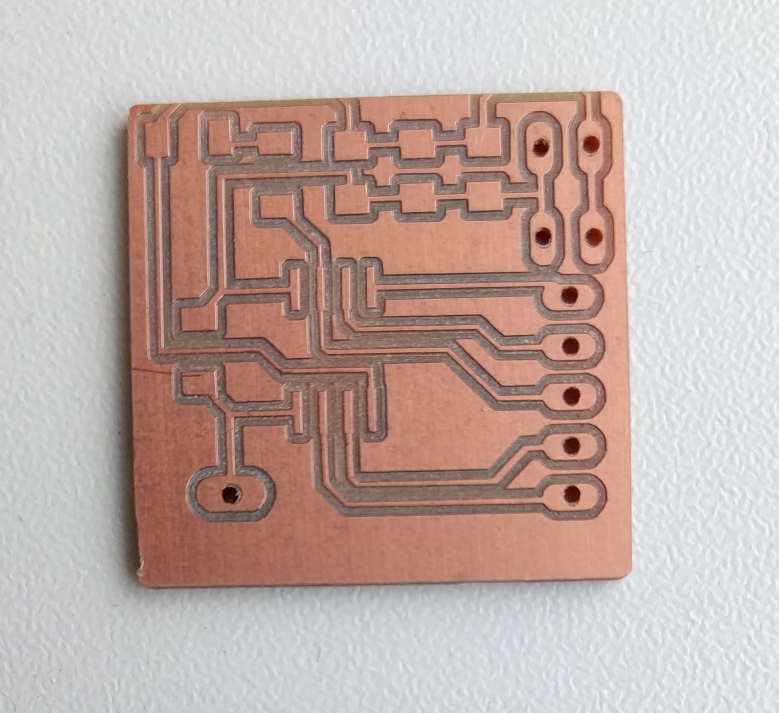
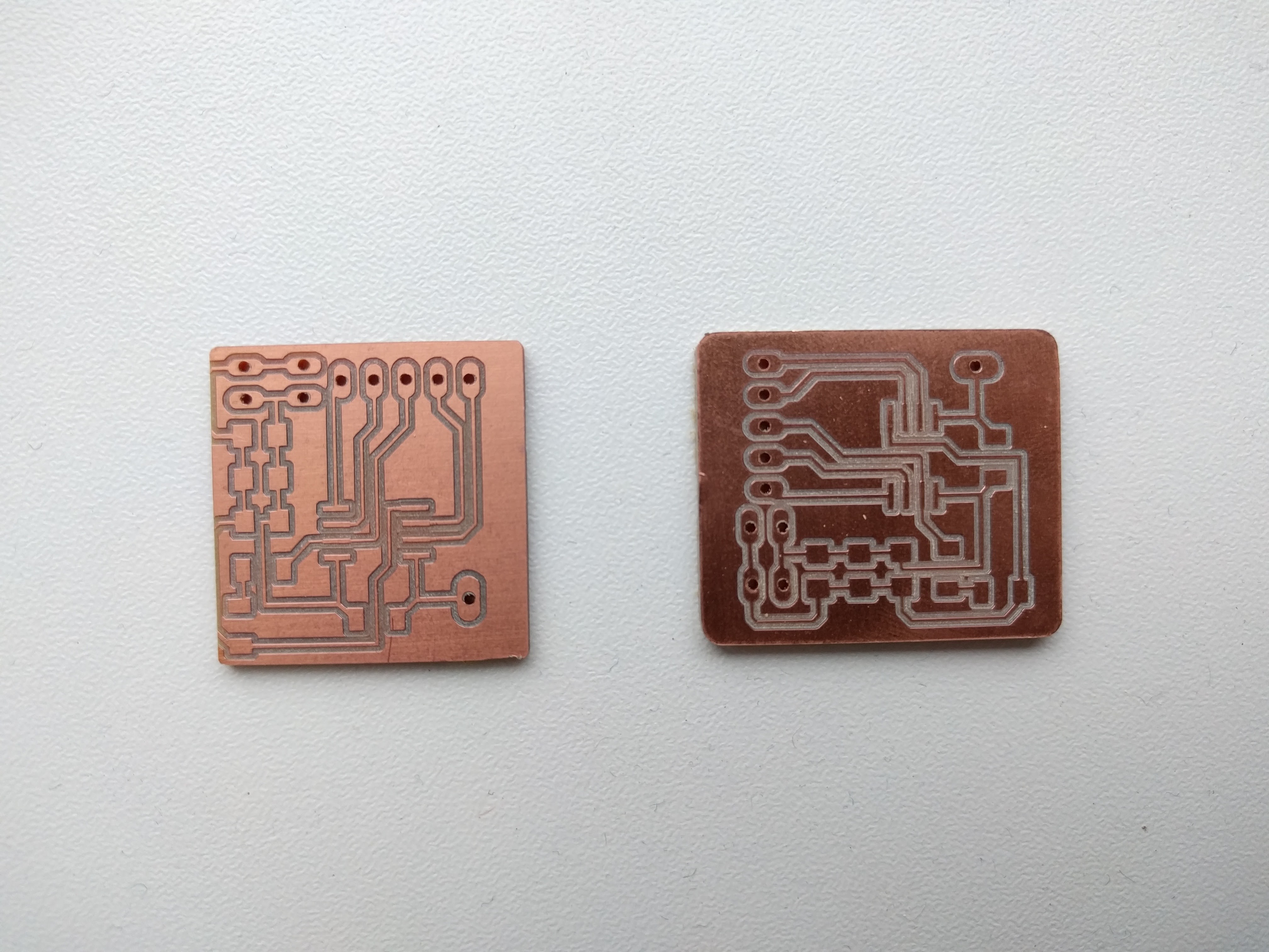
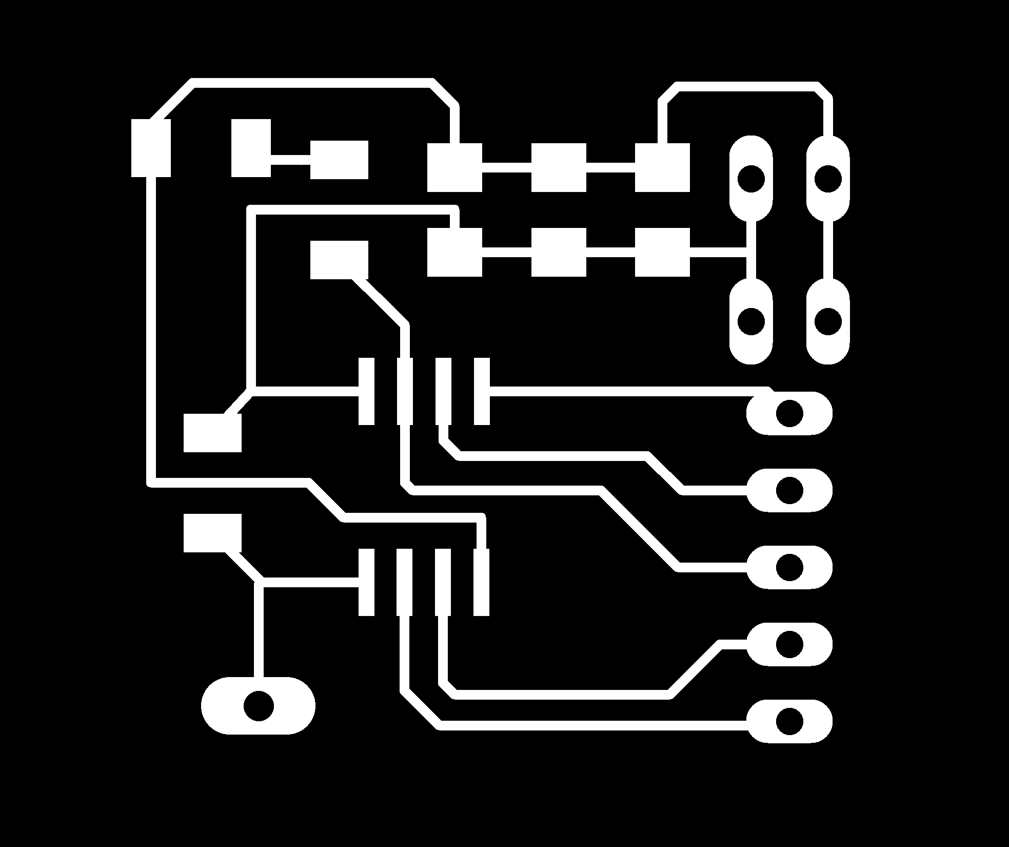
This is how the traces on my second board look like:
There is another a little problem with this second trial, as can be seen from the traces at the bottom right area where the pads for the pin headers are not perfect. This is likely because the PCB was not levelled. However, this is also fixable, so I continue with changing to the 0.3mm tool and setting the new Z-origin to cut the outline of the board:
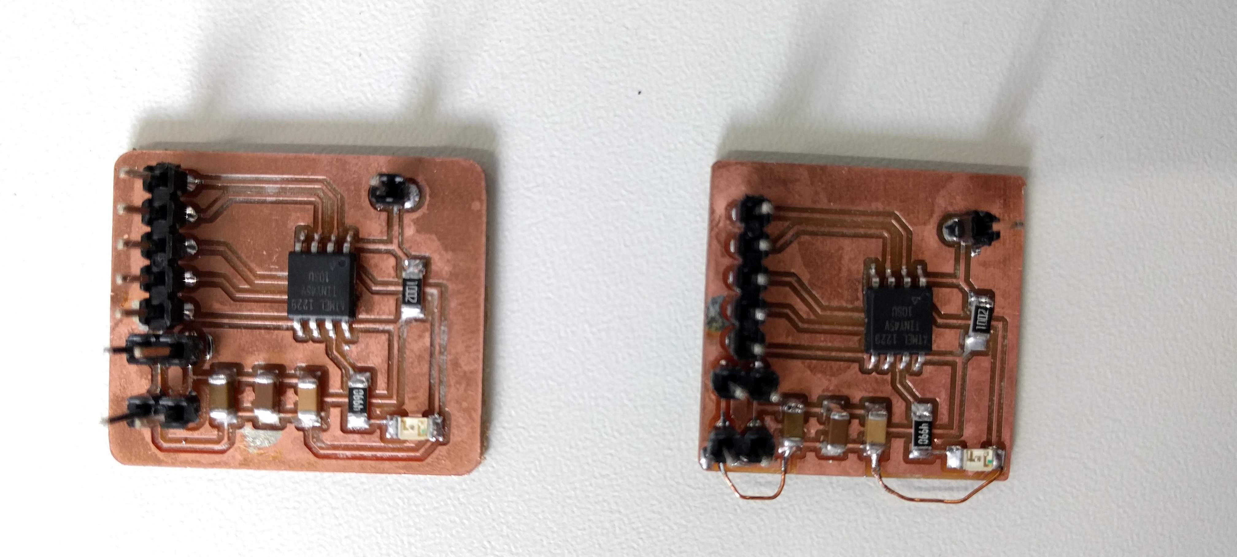
In the end, these are the 2 boards putting next to each other:
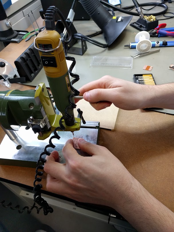
Before populating the PCB, we need to drill the holes for the pin headers on the board using 0.8mm drilling bit:
Afterwards, we follow the PCB pinout image provided by Daniele in order to solder the correct components to the correct positions on the board:
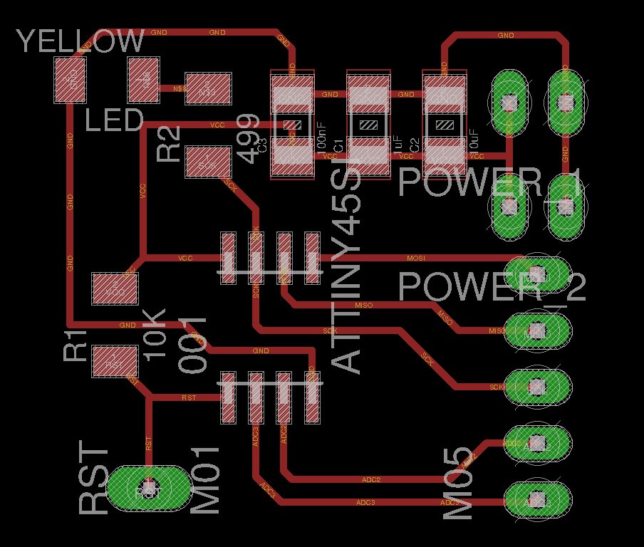
Here are the Bill of Materials for each Hello Board:
1 x ATTiny45 (SOIC8)
                          1 x 1206 SMD LED
                          1 x 1206 499 Ohm SMD Resistor
                          1 x 1206 10K Ohm SMD Resistor
                          1 x 1206 100nF SMD Capacitor
                          1 x 1206 1uF SMD Capacitor
                          1 x 1206 10uF SMD Capacitor
                          1 x 5 Male pin headers
                          2 x 2 Male pin headers
                          1 x 1 Male pin header
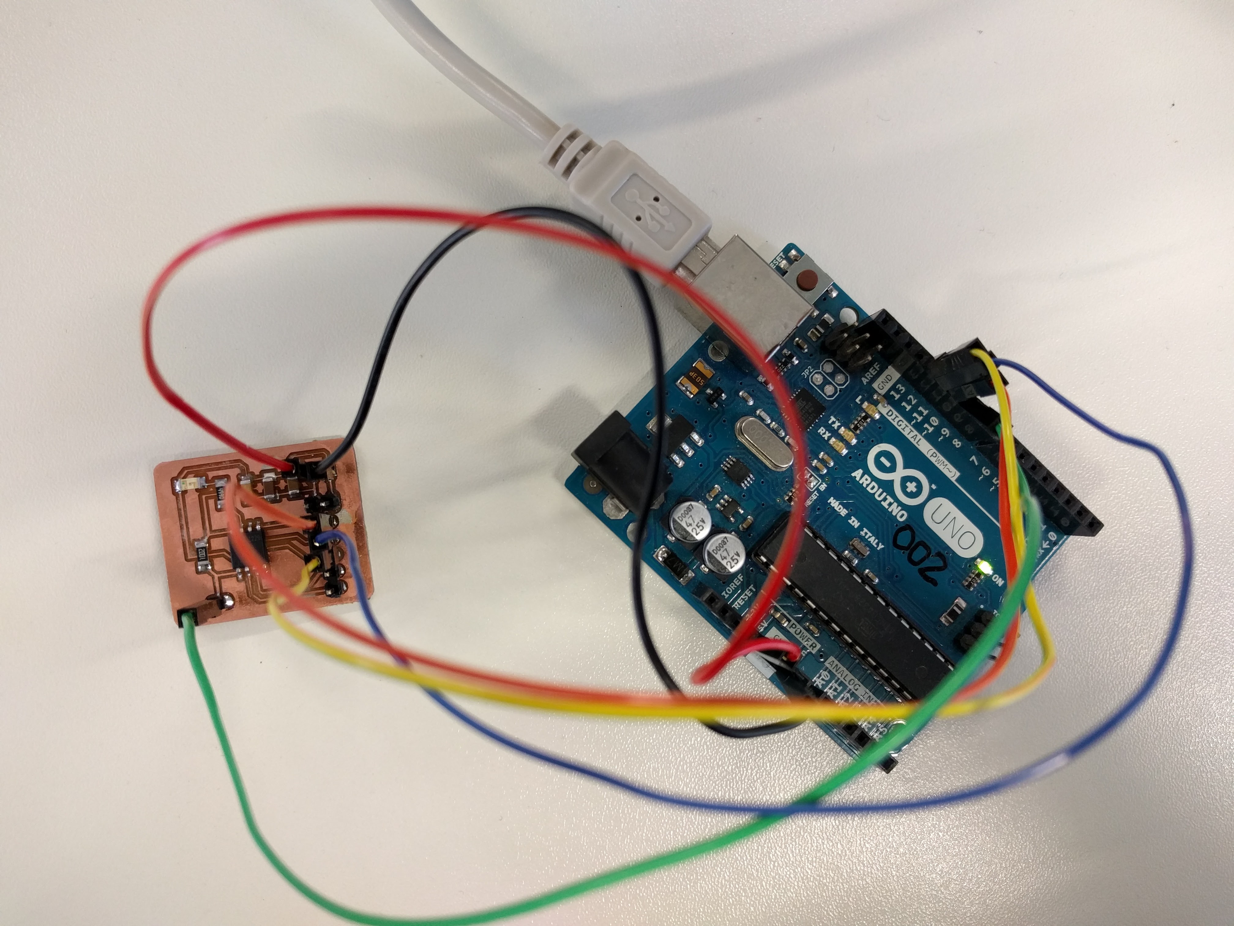
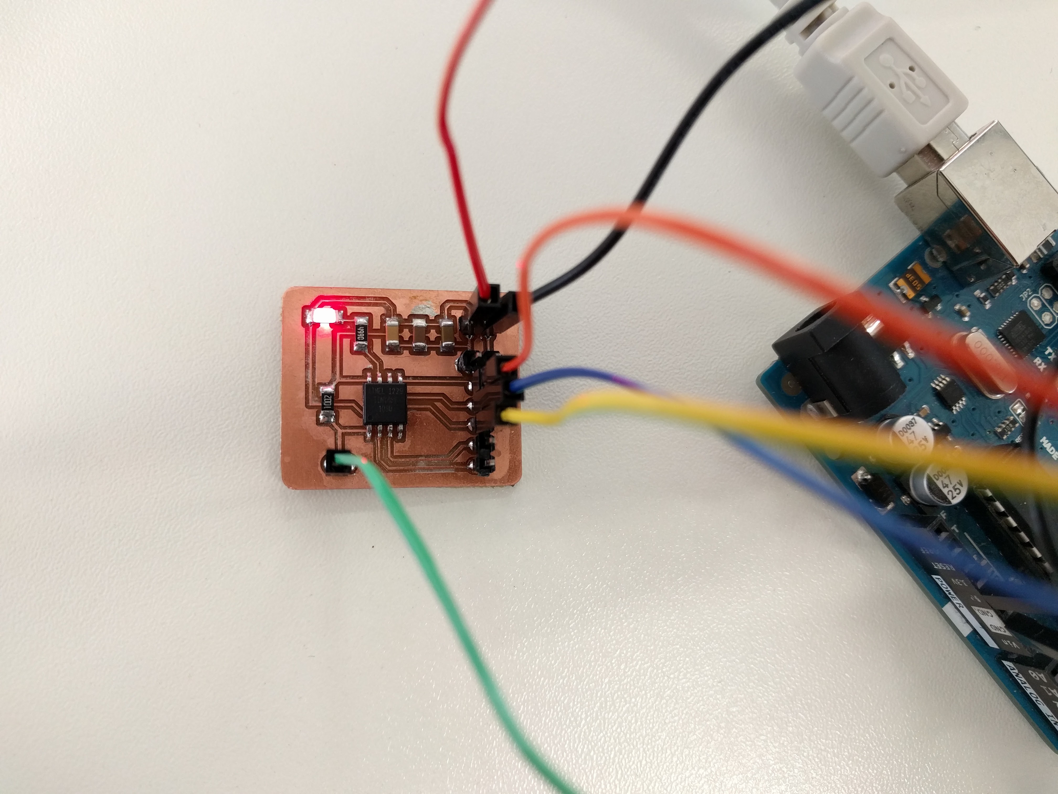
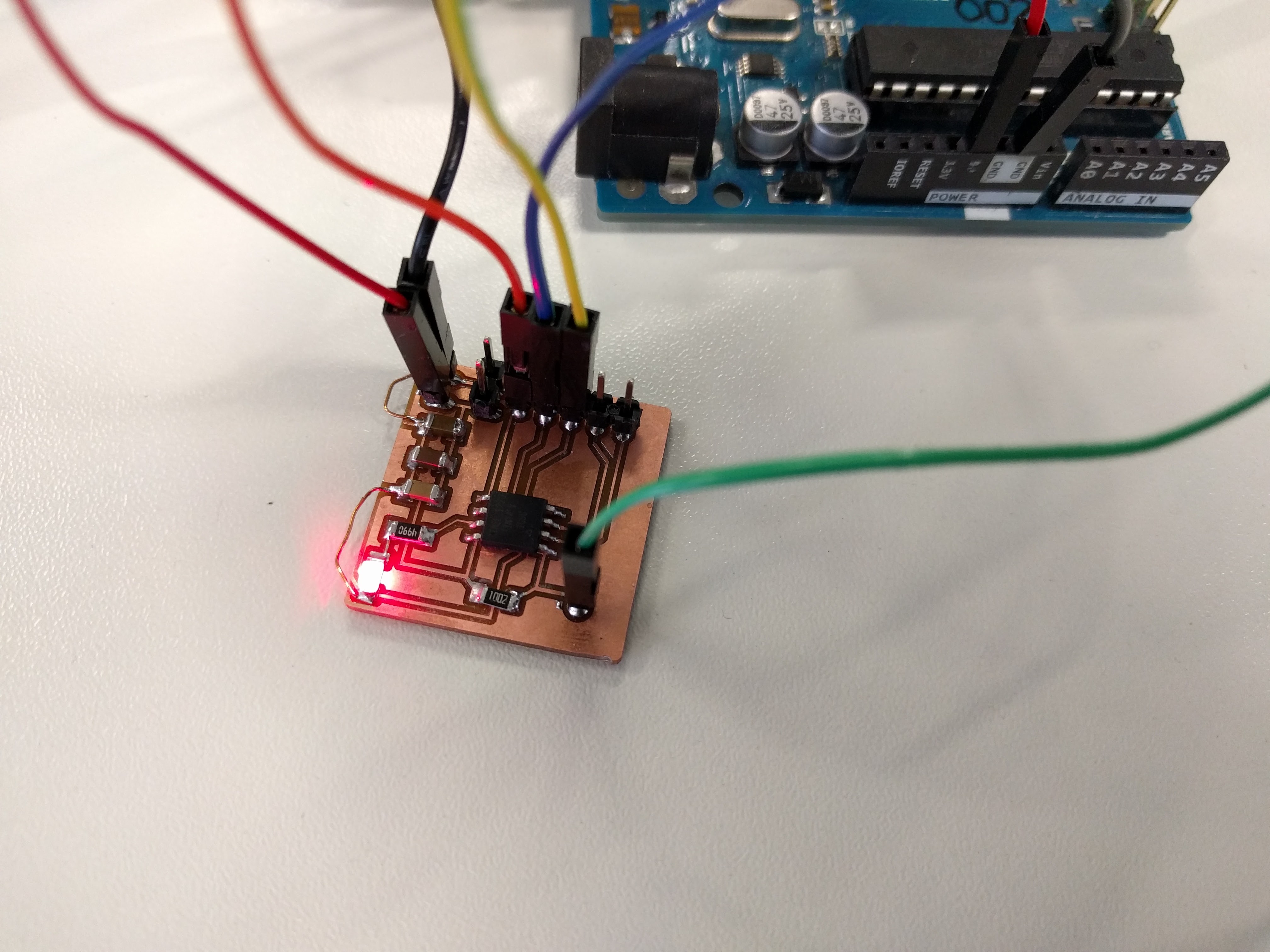
And here are my completed boards (for the first board I need to solder addditional enamelled copper wires to replace the missing traces):
Next, I use the multimeter to check the connections of the board to make sure that the pins on the ATTiny are correctly connected to corresponding pin headers and components and there are no pins accidentally connected together if they should not be.
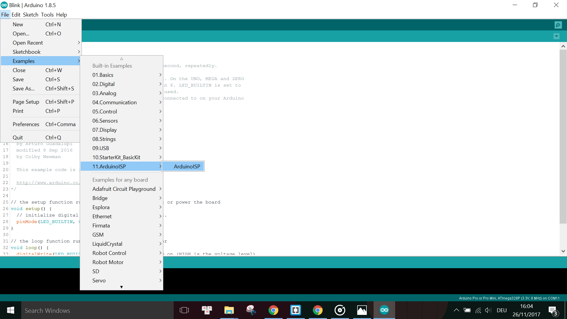
In the Arduino IDE, first I have to upload the ISP programmer sketch to the Arduino Uno under File -> Examples -> Arduino ISP -> ISP:
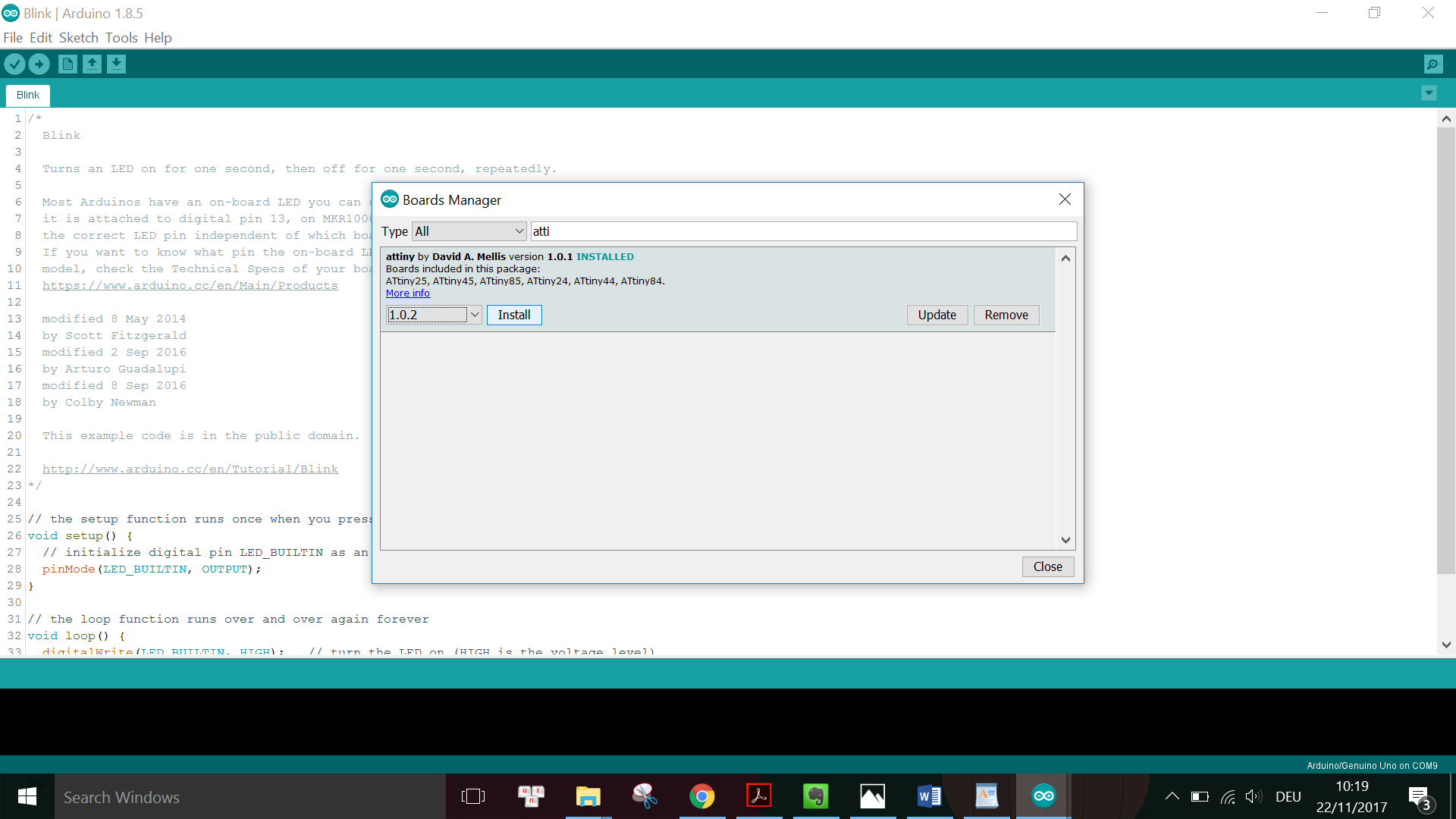
After successfully uploading the ISP sketch to Arduino Uno, I have to add the Board definition for the ATTiny into the IDE in order to program the chip by going to Tools -> Board -> Board Manager and enter "attiny" into the search field. Then I choose the version (usually the newest version) in the dropdown menu and click Install:
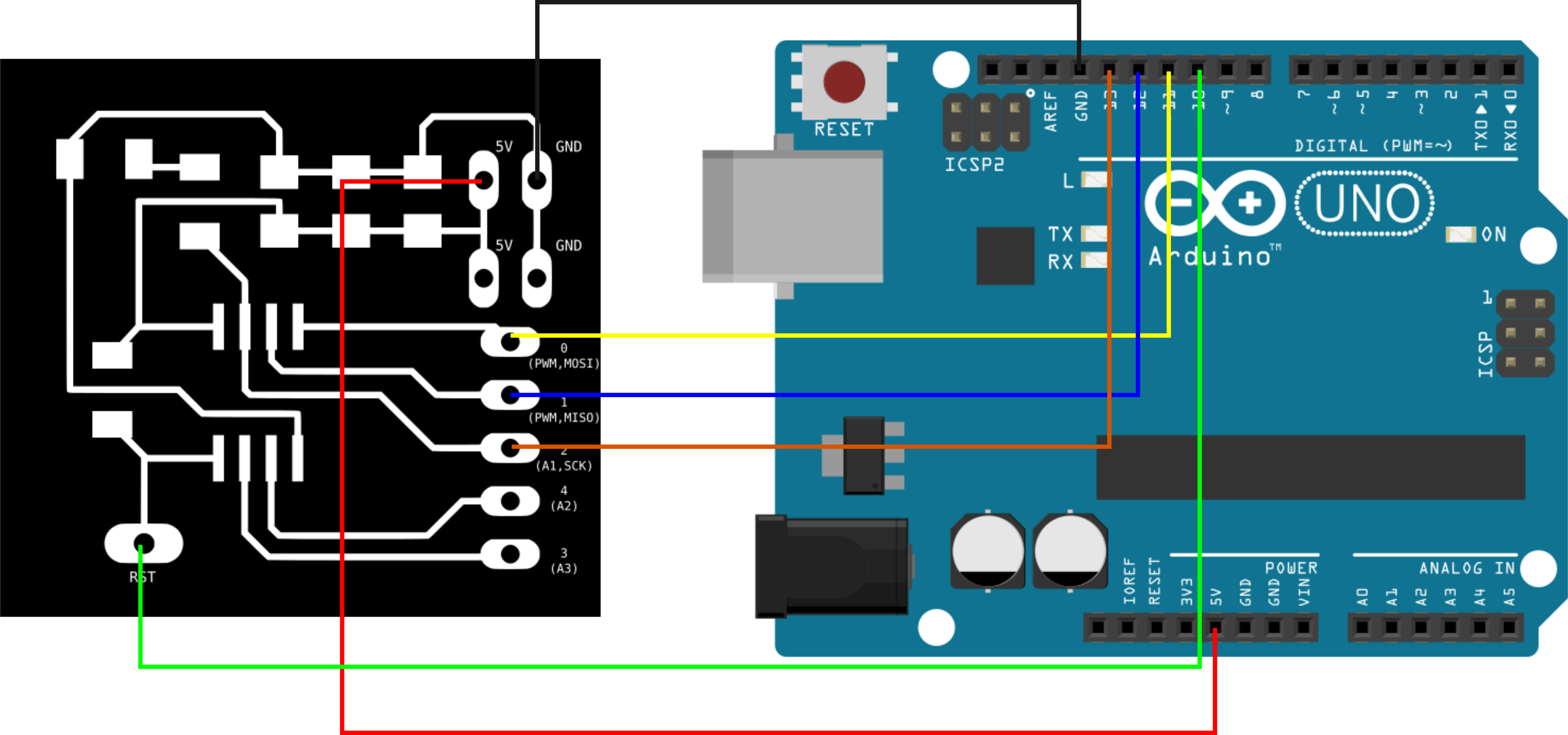
Then I wire the board to the Arduino Uno for programming the ATTiny using the pinout diagram provided by Daniele:
When the board definition is already installed, I go to Tools to choose the correct settings for programming the board as followed:
Board: ATTiny25/45/85
                          Processor: ATTiny45
                          Clock: Internal 8 MHz
                          Port: COM10(Arduino/ Genuino Uno) ##choose the corresponding port
                          Programmer: Arduino as ISP  ##VERY IMPORTANT!!!
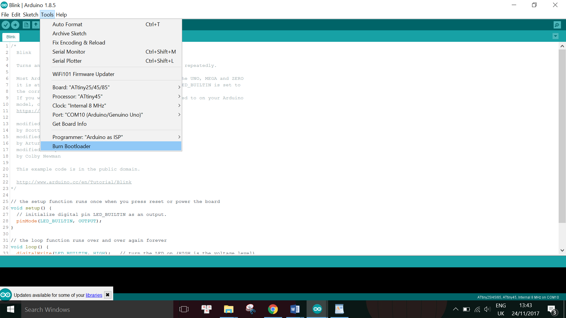
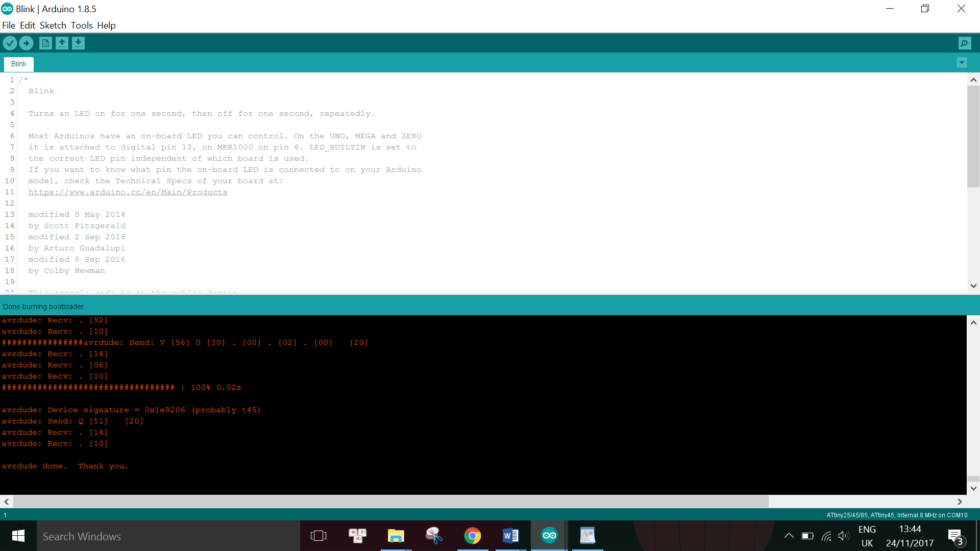
After having the correct settings, I can burn bootloader to the ATTiny by clicking on Tools -> Burn bootloader.
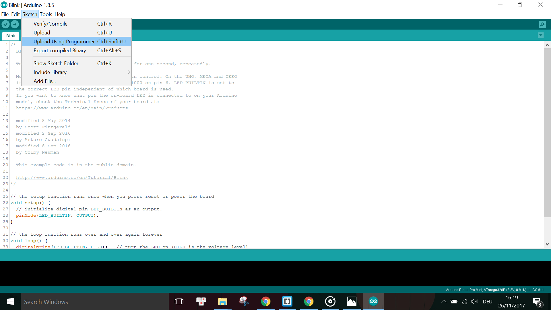
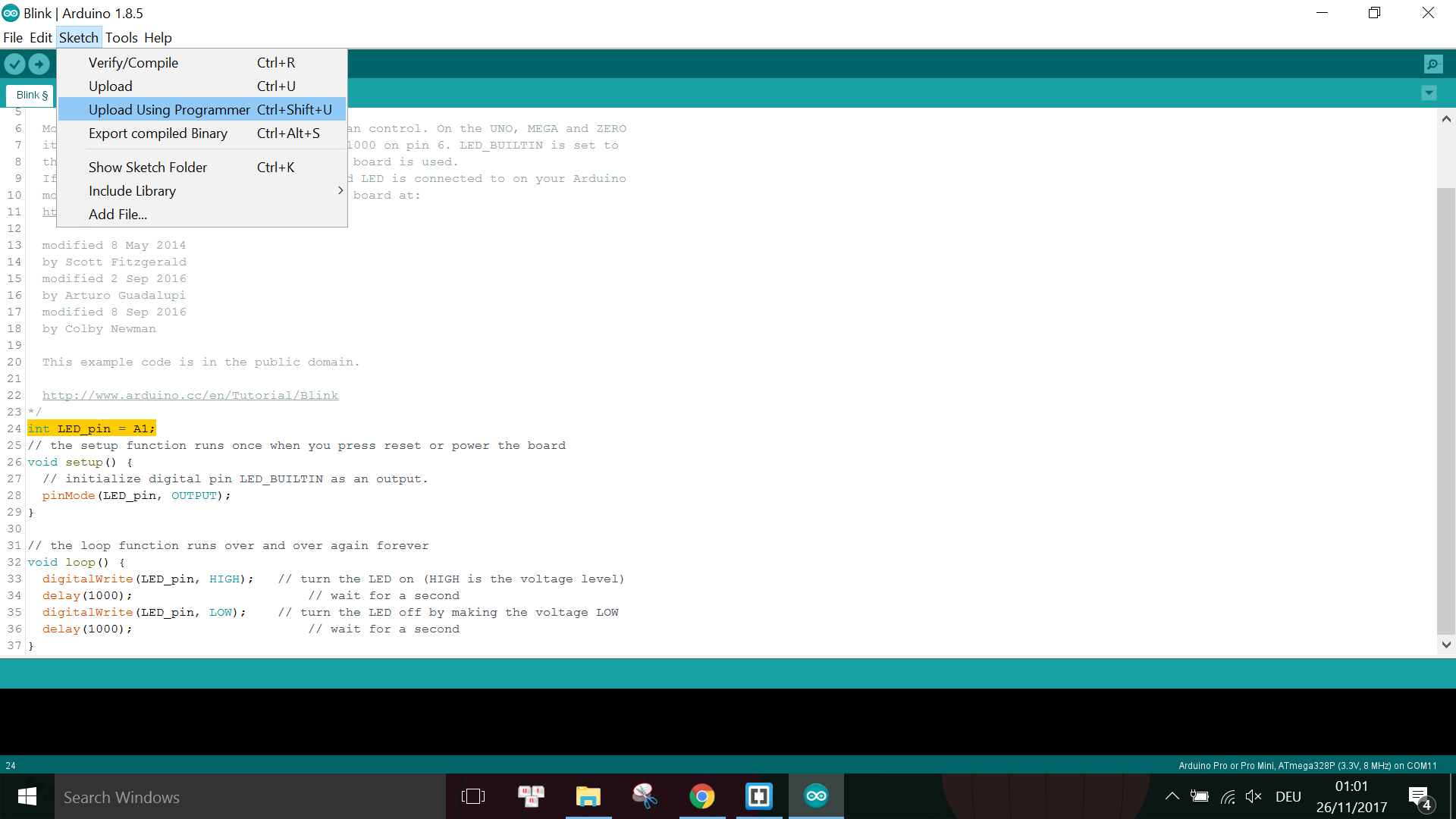
After successfully burning bootloader, I open the example LED blinking sketch under File -> Examples -> Basics -> Blink and go to Sketch -> Upload using programmer to upload the sketch to the ATTiny. IMPORTANT: We should not use the shortcut Upload button else it will override the ISP sketch on the Arduino Uno and then we have to repeat the programming steps all over again.
However, I still get some error messages from the IDE while uploading the sketch to the ATTiny:
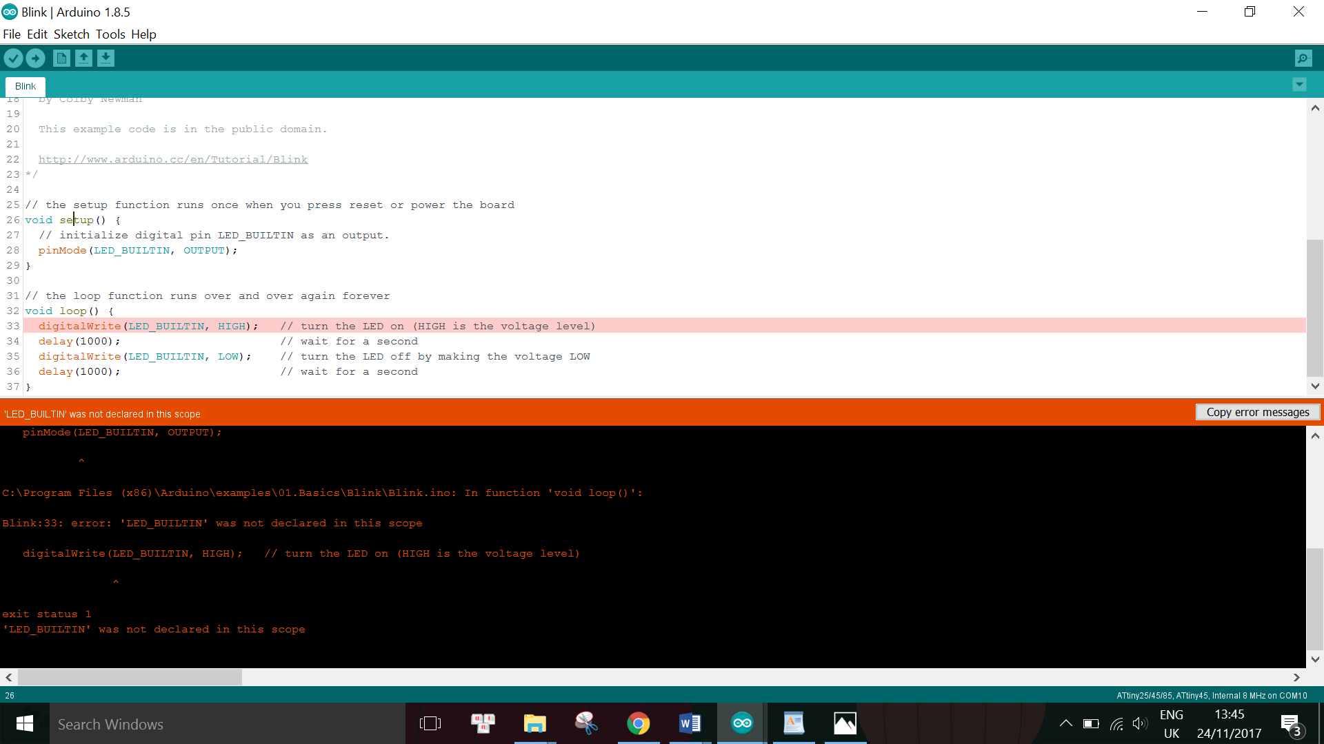
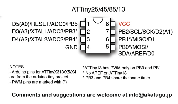
This is because the LED_BUILTIN definition only works for the Arduino Uno-like boards, not for the ATTiny chips. Thus I had to look for the pinout diagram of the ATTiny45 and check the board layout again to figure out that the LED is connected to pin A1 of the chip:
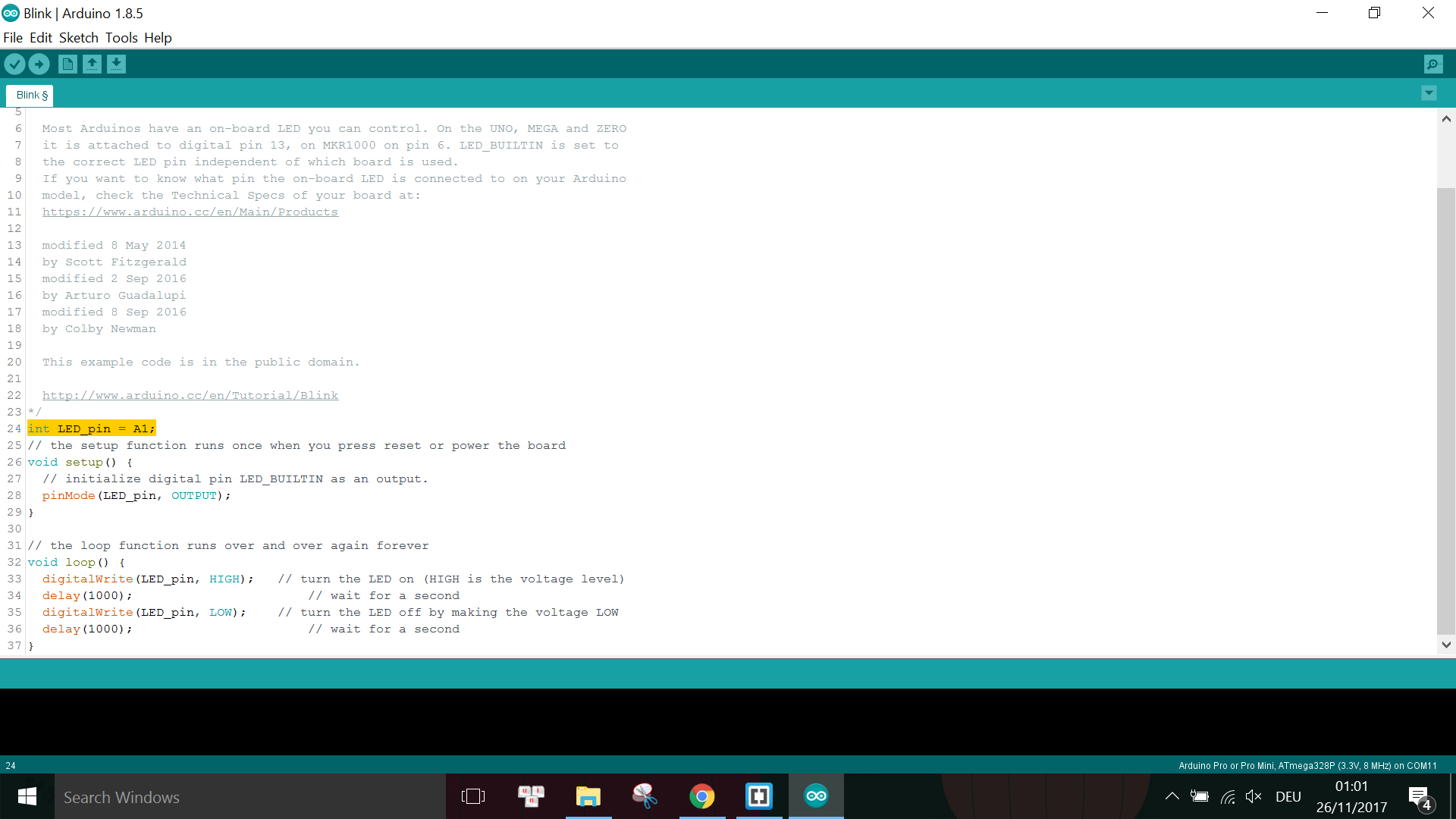
Thus I change the sketch to replace LED_BUILTIN with A1 and upload the sketch again:
And of course now it works perfectly, for both of my boards, YAY!!!
Beside the small problem while uploading the sketch to the ATTiny as described above in Section 3, I encountered some problems with the milling procedure.
When drawing the outline trace for the first board, because the difference between the black and white regions in the image was too small like this,

The Fab Modules software could not produce the complete outline for the board, as seen in the missing line on the left:
As a result, when I tried to mill the outline for my first board, the machine stops halfway and some of the FR2 material was burned at the spot where the spindle stops:
Thus I had to move the spindle away to clean the milling bit as well as the working area and restart the cutting job, and luckily the board was still cut out completely.
However, also because I forgot to use the commands to move the spindle back to XY-origin, and moved it manually instead, the origin point is not exactly the same as the previous job. Thus, some of the traces were also cut out while the machine is cutting the board outline as seen in this image in Section 2.
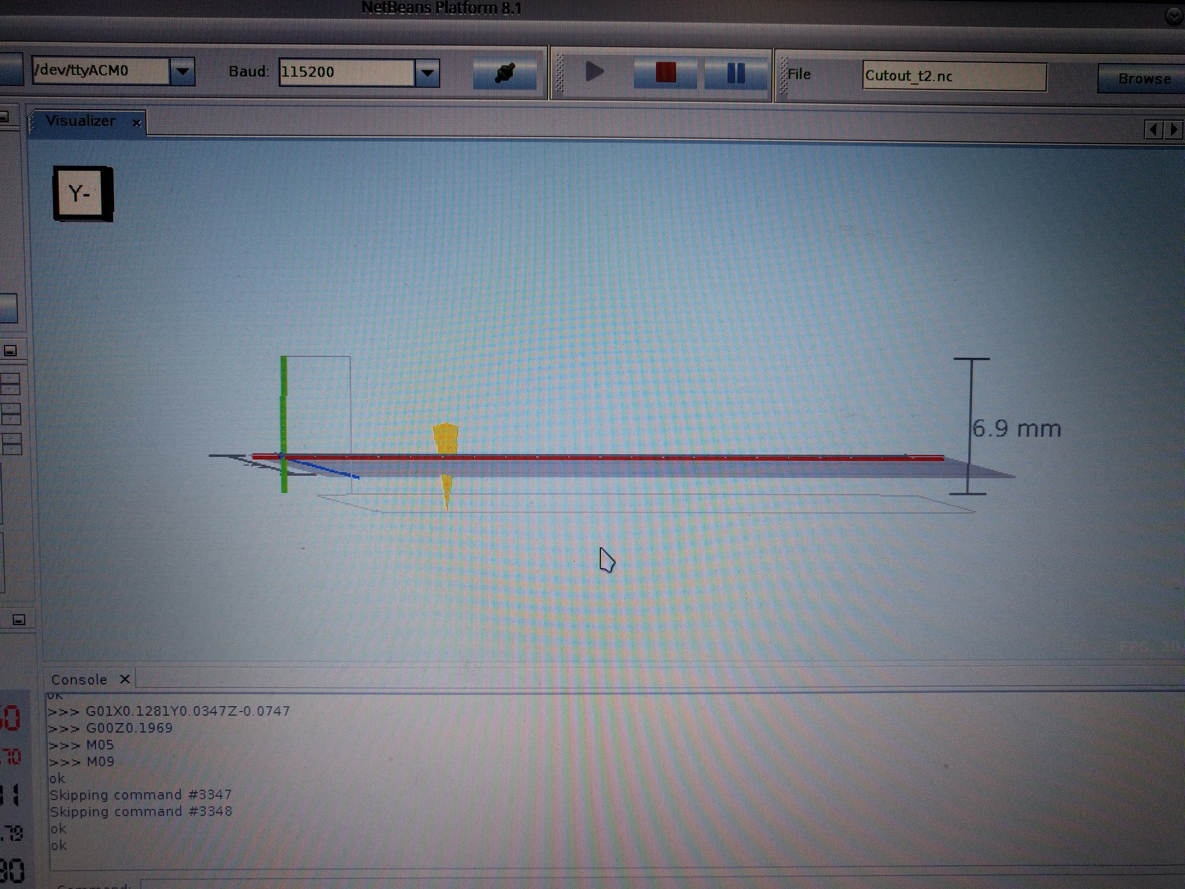
Again, when I tried to cut the second board, although the preview for the cutting job in the CAM processor was fine, when I loaded the G-code into the software, it looked like there was some missing trace again on the right side:
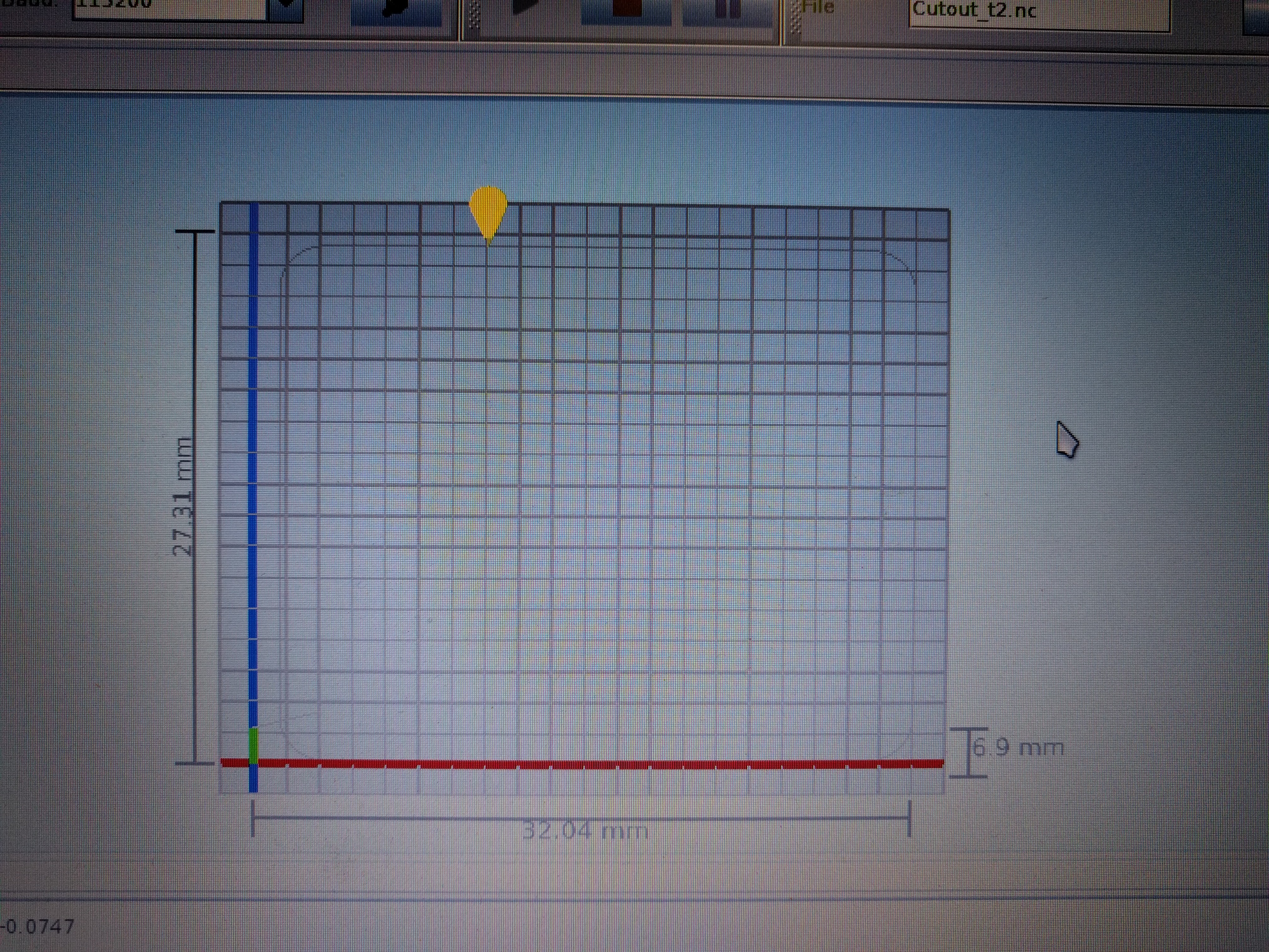
I asked Daniele for help and he suggested that I can try to bring the spindle a little bit (~2mm) up in the Z direction, reset the origin and run the job to see if the spindle is going where it is supposed to. After seeing that the job is correct, I do the calibration of Z-origin again and run the actual cut. Also, I learned afterwards that there is nothing wrong with the G-code and there is no missing trace. It is only because of the grid line overlapping the trace, as can be seen when viewing the trace from another angle:
So milling a PCB has more steps than milling a block of material but basically the key points are to keep the XY-origin and recalibrating the Z origin, because unlike the CAM Processor in Fusion which takes into account the difference in the Body lengths of the different end tools, the Fab Modules CAM Processor does not have this option. Also, for the Cirqoid it is more complicated because we have to manually enter commands for moving the spindle to XY-origin while for the Roland we have buttons for that, thus I keep forgetting this part. Otherwise, with more practice it should get better.